\n
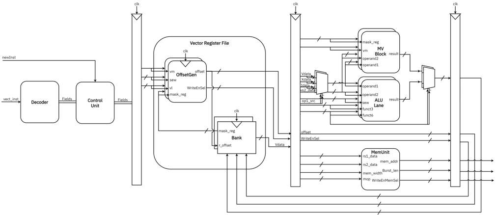
## Diagram: Vector Processor Block Diagram
### Overview
The image depicts a block diagram of a vector processor architecture. It illustrates the interconnection of several key components, including a Decoder, Control Unit, Vector Register File, Offset Generator, MV Block, ALU Lane, and MemUnit. The diagram focuses on data flow and control signals within the processor.
### Components/Axes
The major components are:
* **Decoder:** Receives `vect_inst` input and outputs `Fields`.
* **Control Unit:** Receives `Fields` input and outputs control signals.
* **Vector Register File:** Contains `vm`, `offset`, `new`, `mask_reg`, `WriteEnSel`, `vdata`. It has a `Bank` component.
* **Offset Generator:** Receives `vm`, `offset`, `new` and outputs `offset`.
* **MV Block:** Receives `mask_reg`, `result`, `operand1`, `operand2`.
* **ALU Lane:** Receives `operand1`, `operand2`, `op1_src`, `funct6`, `funct5`, `funct3` and outputs `result`.
* **MemUnit:** Receives `s1_data`, `mem_addr`, `mem_width`, `Burst_len`, `mop`, `WriteEnMemSel` and outputs data.
Key signals/connections:
* `vect_inst`
* `Fields`
* `clk` (clock signal, present at multiple locations)
* `vm`
* `offset`
* `new`
* `mask_reg`
* `WriteEnSel`
* `vdata`
* `op1_src`
* `funct3`, `funct5`, `funct6`
* `s1_data`
* `mem_addr`
* `mem_width`
* `Burst_len`
* `mop`
* `WriteEnMemSel`
* `operand1`, `operand2`, `result`
### Detailed Analysis or Content Details
The diagram shows a data flow from left to right.
1. **Decoder & Control Unit:** The `vect_inst` signal enters the Decoder, which extracts `Fields`. These `Fields` are then fed into the Control Unit, which generates various control signals.
2. **Vector Register File & Offset Generation:** The Control Unit sends signals to the Vector Register File, controlling access to `vm`, `offset`, `new`, `mask_reg`, and `vdata`. The `vm`, `offset`, and `new` signals are also inputs to the Offset Generator, which outputs an `offset` signal.
3. **MV Block & ALU Lane:** The Vector Register File provides `mask_reg` to the MV Block. The ALU Lane receives `operand1` and `operand2` and control signals (`op1_src`, `funct3`, `funct5`, `funct6`) to perform an operation, outputting `result`.
4. **MemUnit:** The MemUnit receives `s1_data`, `mem_addr`, `mem_width`, `Burst_len`, `mop`, and `WriteEnMemSel` signals.
The diagram also shows multiple clock signals (`clk`) distributed to the Vector Register File, MV Block, and other components, indicating synchronous operation. The `newfast` signal is connected to the Decoder and Control Unit.
### Key Observations
* The diagram is highly interconnected, suggesting a complex control structure.
* The presence of multiple clock signals indicates a synchronous design.
* The `mask_reg` signal is used in both the MV Block and the Vector Register File, suggesting a masking operation is supported.
* The MemUnit is positioned at the rightmost side, indicating memory access is a key function of this processor.
* The diagram does not provide specific numerical values or performance metrics. It is a structural representation of the processor.
### Interpretation
This diagram represents a simplified architecture of a vector processor. The key idea is to perform the same operation on multiple data elements simultaneously, leveraging the parallelism inherent in vector processing. The Vector Register File stores the vector data, while the ALU Lane performs the arithmetic or logical operations. The MemUnit handles data transfer between memory and the registers. The Control Unit orchestrates the entire process based on the decoded instruction (`vect_inst`).
The presence of `mask_reg` suggests that the processor supports conditional operations, where only certain elements of the vector are processed based on the mask. The `offset` signal indicates that the processor can access elements of the vector with an offset, potentially for strided access patterns.
The diagram is a high-level representation and does not detail the internal implementation of each block. It serves as a blueprint for understanding the overall structure and data flow of the vector processor. The diagram does not provide any performance data or specific implementation details, so it is difficult to assess the efficiency or capabilities of the processor based solely on this diagram. It is a structural description, not a behavioral one.