TECHNICAL ASSET FINGERPRINT
06a29041320ce4bff744f9e6
Click to view fullscreen
Press ESC or click to close
FOUND IN PAPERS
EXPERT: healer-alpha-free VERSION 1
RUNTIME: free/openrouter/healer-alpha
INTEL_VERIFIED
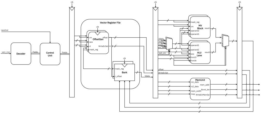
## Diagram: Vector Processing Unit Microarchitecture
### Overview
The image is a detailed block diagram illustrating the microarchitecture of a vector processing unit, likely for a RISC-V vector extension implementation. It shows the data and control flow from instruction fetch/decode through to execution and memory access. The diagram is organized into three main vertical sections separated by pipeline registers (vertical bars with clock inputs).
### Components/Axes
**Left Section (Instruction Decode & Control):**
- **Inputs:** `newInst` (top), `vect_inst` (bottom left)
- **Components:**
- `Decoder`: Receives `vect_inst`. Outputs `Fields` to the Control Unit.
- `Control Unit`: Receives `Fields` from Decoder and `newInst`. Outputs `Fields` to the central section.
- **Pipeline Register:** A vertical bar with a `clk` input at the top, separating the left and central sections.
**Central Section (Vector Register File & Address Generation):**
- **Main Component:** `Vector Register File` (large rounded rectangle).
- **Sub-components within Vector Register File:**
- `OffsetGen`: Receives `clk`, `sew`, `vl`, `mask_reg`. Outputs `offset`.
- `Bank`: Receives `clk`, `mask_reg`, `r_offset`. Outputs `Vldata`.
- **Signals:** `WriteEnSel` is an input to the Vector Register File.
- **Pipeline Register:** A second vertical bar with a `clk` input, separating the central and right sections.
**Right Section (Execution & Memory Units):**
- **Top Execution Path:**
- `MV Block`: Receives `mask_reg`, `vm`, `operand2`, `operand1`. Outputs `result`.
- A multiplexer (trapezoid) selects between the `MV Block` result and the `ALU Lane` result.
- **Middle Execution Path:**
- `ALU Lane`: Receives `operand1`, `operand2`, `sew`, `funct3`, `funct6`. Outputs `result`.
- A multiplexer before the ALU Lane selects inputs from `vdata`, `s1_data`, `s2_data`, `vl`, `vtype`, `vl`, `vtype` based on `op1_src`.
- **Bottom Memory Path:**
- `MemUnit`: Receives `s1_data`, `s2_data`, `mem_width`, `mop`. Outputs `mem_addr`, `Burst_len`, `WriteEnMemSel`.
- **Signals:** `offset` and `WriteEnSel` from the central section are routed to the right section.
- **Pipeline Register:** A third vertical bar with a `clk` input on the far right.
- **Outputs:** Multiple output arrows on the far right, including from the final multiplexer and the `MemUnit`.
**Global Signals:**
- `clk`: Clock signal, fed into all three pipeline registers and sub-components like `OffsetGen` and `Bank`.
- `mask_reg`: A register value flowing from the Vector Register File to the `MV Block` and `Bank`.
- `Vldata`: Data output from the Vector Register File's `Bank`, sent to the multiplexer before the `ALU Lane`.
### Detailed Analysis
**Component Isolation & Flow:**
1. **Header / Instruction Stage (Left):** The process begins with a vector instruction (`vect_inst`) entering the `Decoder`. The decoder extracts fields and passes them to the `Control Unit`, which also receives a `newInst` signal. The control unit generates further control fields that cross the first pipeline register.
2. **Central / Register & Address Stage:** The control fields enter the `Vector Register File`. Inside, the `OffsetGen` unit calculates an `offset` using parameters like `sew` (standard element width) and `vl` (vector length). The `Bank` unit reads register data (`Vldata`) using a register offset (`r_offset`) and a mask (`mask_reg`). The `WriteEnSel` signal controls write enables.
3. **Right / Execution & Memory Stage:** Data and control cross the second pipeline register.
* **Move/Logic Path:** The `MV Block` performs operations, potentially for mask or move instructions.
* **ALU Path:** A multiplexer selects the first operand (`operand1`) for the `ALU Lane` from various sources (`vdata`, `s1_data`, etc.). The ALU performs operations based on `funct3` and `funct6` codes.
* **Memory Path:** The `MemUnit` handles load/store operations, generating memory addresses (`mem_addr`) and burst lengths (`Burst_len`).
* A final multiplexer selects the result from either the `MV Block` or the `ALU Lane` path. The output, along with memory signals, crosses the final pipeline register.
**Spatial Grounding:**
- The **legend/labels** are embedded directly next to or inside their respective component boxes.
- The **pipeline registers** are positioned as vertical dividers at approximately 25% and 65% of the diagram's width from the left.
- The **Vector Register File** is the central, dominant component.
- The **execution units** (`MV Block`, `ALU Lane`) are stacked vertically in the top-right quadrant.
- The **MemUnit** is isolated in the bottom-right quadrant.
### Key Observations
1. **Pipelined Architecture:** The three prominent `clk`-driven pipeline registers indicate a deeply pipelined design, separating decode, register fetch, and execute/memory stages for high throughput.
2. **Dual Execution Paths:** The design features separate, parallel paths for what appear to be mask/move operations (`MV Block`) and standard arithmetic/logic operations (`ALU Lane`), suggesting optimization for different instruction types.
3. **Complex Operand Selection:** The multiplexer feeding the `ALU Lane` has many inputs (`vdata`, `s1_data`, `s2_data`, `vl`, `vtype`), indicating flexible operand sourcing, possibly for different addressing modes or immediate values.
4. **Integrated Memory Unit:** The `MemUnit` is tightly coupled with the execution pipeline, receiving data directly and outputting control signals, characteristic of a load/store unit within a vector processor.
5. **Control and Data Path Separation:** The diagram clearly separates the control flow (left side, `Control Unit`) from the data path (central and right sides), a classic computer architecture design principle.
### Interpretation
This diagram represents the **data path and control flow of a RISC-V Vector Extension (RVV) compatible processing unit**. The components map directly to RVV concepts:
- `sew`, `vl`, `vtype` are standard RISC-V vector configuration parameters.
- The `Vector Register File` with `OffsetGen` and `Bank` implements the large, configurable vector register file and the indexed/strided access patterns defined by RVV.
- The `MV Block` likely handles vector mask operations and register-to-register moves.
- The `ALU Lane` is the core computational unit for element-wise operations.
- The `MemUnit` implements the complex vector load/store operations with burst control.
The architecture is designed for **high-performance, pipelined execution of vector instructions**. The separation of mask and data paths, flexible operand selection, and dedicated memory unit are all optimizations to handle the high data-level parallelism inherent in vector processing. The multiple pipeline stages suggest this unit is intended to run at a high clock frequency, with each stage performing a small, manageable part of the overall vector instruction execution. The design balances flexibility (many mux inputs) with dedicated hardware for common operations (separate MV and ALU blocks).
DECODING INTELLIGENCE...