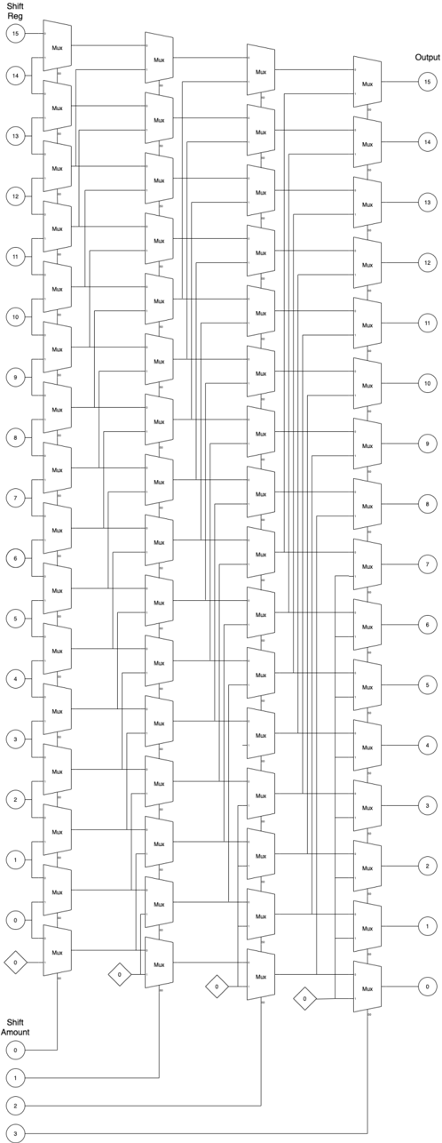
## Digital Circuit Diagram: 16-bit Barrel Shifter Implementation
### Overview
The image displays a detailed schematic diagram of a digital circuit, specifically a 16-bit barrel shifter implemented using a network of multiplexers (Mux). The circuit is designed to shift a 16-bit input vector (`Shift Reg`) by a variable number of positions (0 to 15) as determined by a 4-bit control input (`Shift Amount`). The data flows from left to right.
### Components/Axes
* **Primary Components:** The diagram consists of a grid of identical 2-to-1 multiplexer (Mux) symbols. Each Mux has two data inputs, one select input (indicated by a small triangle on the side), and one output.
* **Input Labels (Left Side):** A vertical column of numbered circles from **0** (bottom) to **15** (top), labeled collectively as `Shift Reg`. These represent the 16 input bits.
* **Output Labels (Right Side):** A vertical column of numbered circles from **0** (bottom) to **15** (top), labeled collectively as `Output`. These represent the 16 output bits after the shift operation.
* **Control Inputs (Bottom):** Four input lines labeled `Shift Amount`, with individual bits labeled **0**, **1**, **2**, and **3** from top to bottom. These form a 4-bit binary number controlling the shift distance.
* **Ground/Zero Connections:** Diamond-shaped symbols containing the number **0** are present at the bottom of each column of Muxes, indicating a logical '0' or ground connection for certain Mux inputs.
* **Wiring:** A complex network of lines connects the inputs, Muxes, control signals, and outputs. The wiring pattern is systematic, with each stage of Muxes controlled by a different bit of the `Shift Amount`.
### Detailed Analysis
**Circuit Structure and Flow:**
1. **Input Stage:** The 16 bits of `Shift Reg` (0-15) are fed into the first (leftmost) column of multiplexers.
2. **Shifting Stages:** The circuit is organized into four vertical columns of Muxes. Each column corresponds to one bit of the `Shift Amount` control:
* **Column 1 (Leftmost):** Controlled by `Shift Amount` bit **0**. This stage handles a conditional shift of **1 position**.
* **Column 2:** Controlled by `Shift Amount` bit **1**. This stage handles a conditional shift of **2 positions**.
* **Column 3:** Controlled by `Shift Amount` bit **2**. This stage handles a conditional shift of **4 positions**.
* **Column 4 (Rightmost):** Controlled by `Shift Amount` bit **3**. This stage handles a conditional shift of **8 positions**.
3. **Output Stage:** The outputs from the final column of Muxes are directly connected to the `Output` pins (0-15).
**Multiplexer Logic:**
* Each Mux in a column has its select line connected to the same bit of the `Shift Amount`.
* For a given Mux, one data input comes from the previous stage (or the original input for the first column). The other data input is wired to a different bit position from the previous stage, implementing the shift.
* **Example (Shift by 1):** In the first column, the Mux for Output bit `n` will select either Input bit `n` (if Shift Amount bit 0 = 0, no shift) or Input bit `n-1` (if Shift Amount bit 0 = 1, shift left by 1). Input bit `0`'s Mux in this column takes its second input from the `0` diamond (ground), implementing a shift-in of zero.
* This pattern cascades through the stages. The final output is the result of applying up to four conditional shifts (of 1, 2, 4, and 8 positions) in sequence, allowing any shift amount from 0 to 15.
**Spatial Grounding of Key Elements:**
* **Legend/Labels:** Input labels are aligned vertically on the far left. Output labels are aligned vertically on the far right. Control labels are at the bottom left.
* **Control Signal Routing:** The line from `Shift Amount` bit **0** runs horizontally to the right, connecting to the select input of every Mux in the first column. Similarly, bit **1** connects to the second column, bit **2** to the third, and bit **3** to the fourth.
* **Zero/Ground Symbols:** The diamond `0` symbols are placed at the bottom of each Mux column, providing the shift-in value for the lowest bit in each stage.
### Key Observations
1. **Systematic Wiring:** The interconnections follow a precise, repeating pattern characteristic of a logarithmic barrel shifter. The wiring density increases in the middle columns due to the larger shift distances (2 and 4 positions).
2. **No External Clock:** This is a purely combinational logic circuit. The output changes asynchronously in response to changes in the `Shift Reg` or `Shift Amount` inputs.
3. **Complete 16-bit Coverage:** The circuit can perform any cyclic or logical shift (depending on the interpretation of the `0` inputs) within a 16-bit word.
4. **Scalability Pattern:** The design demonstrates a scalable architecture. A 32-bit shifter would require an additional stage controlled by a 5th shift amount bit (shift of 16).
### Interpretation
This diagram is a gate-level representation of a fundamental digital building block. A barrel shifter is crucial in processors for executing shift/rotate instructions efficiently in a single clock cycle, and in hardware for data alignment, normalization in floating-point units, and cryptographic algorithms.
The circuit's operation can be understood as a binary decomposition of the shift amount. For example, to shift by **5 positions** (binary `0101`):
1. Bit 0 is 1: The first stage shifts by 1.
2. Bit 1 is 0: The second stage does not shift.
3. Bit 2 is 1: The third stage shifts by 4.
4. Bit 3 is 0: The fourth stage does not shift.
The net result is a shift of 1 + 4 = 5 positions.
The use of multiplexers at each stage makes the design regular and suitable for VLSI implementation. The `0` inputs suggest this is a **logical shifter**, where bits shifted in are zeros, as opposed to a **circular (rotate) shifter** where bits shifted out are fed back into the opposite end. The diagram provides all necessary information to synthesize this circuit in a hardware description language (HDL) like Verilog or VHDL.