## Digital Circuit Diagram: Configurable Shift Register/Multiplexer Array
### Overview
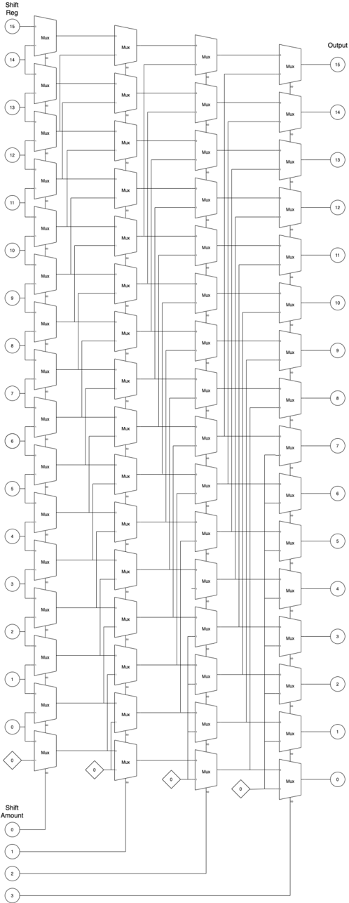
The diagram depicts a complex digital circuit architecture featuring a grid of multiplexer (Mux) blocks arranged in a 16x4 matrix. The system includes labeled input registers ("Shift Reg"), configurable shift amounts, and output registers. The structure suggests a programmable data routing system with bit-level control.
### Components/Axes
1. **Vertical Axis (Left Side):**
- Labeled "Shift Reg" at the top
- 16 numbered registers (15-0) descending vertically
- Each register feeds into a column of Mux blocks
2. **Horizontal Axis (Bottom):**
- Labeled "Shift Amount" with values 0, 1, 2, 3
- Four columns of Mux blocks corresponding to shift values
3. **Output Section (Right Side):**
- 16 output registers (15-0) mirroring input numbering
- Each output register receives processed data from Mux blocks
4. **Mux Blocks:**
- 64 total Mux elements (16 rows × 4 columns)
- Each Mux has two inputs (A/B) and one output (Y)
- Control signals not explicitly labeled but implied by shift amount
### Detailed Analysis
1. **Input Stage:**
- 16-bit "Shift Reg" provides initial data
- Each bit (15-0) feeds into the first column of Mux blocks
2. **Processing Stage:**
- Four parallel Mux columns process data based on shift amount
- Column 0 (shift=0): Direct passthrough
- Column 1 (shift=1): Shifts data right by 1 bit
- Column 2 (shift=2): Shifts data right by 2 bits
- Column 3 (shift=3): Shifts data right by 3 bits
- Mux selection logic determined by shift amount value
3. **Output Stage:**
- Final outputs mirror input numbering (15-0)
- Each output bit receives processed data from corresponding Mux column
- Output configuration depends on selected shift amount
### Key Observations
1. **Bit Positioning:**
- Higher-numbered bits (15-12) occupy top positions
- Lower-numbered bits (3-0) occupy bottom positions
- Consistent numbering across input/output stages
2. **Shift Behavior:**
- Shift amount 0: No change in bit positions
- Shift amount 1: Each bit moves to position n-1
- Shift amount 3: Bits 3-0 shift out of range (likely zero-padded)
3. **Control Mechanism:**
- Shift amount selector likely uses binary encoding (00, 01, 10, 11)
- No explicit control signals shown for Mux selection
### Interpretation
This diagram represents a configurable bit-shifting system with programmable delay/routing capabilities. The architecture allows:
- **Data Preservation:** Shift amount 0 maintains original bit positions
- **Temporal Delay:** Higher shift amounts create progressive delays
- **Bit Isolation:** Individual bit control through Mux configuration
- **Parallel Processing:** Four simultaneous shift operations
The system appears designed for applications requiring:
- Configurable data pipelines
- Bit-level signal manipulation
- Parallel shift operations
- Programmable delay elements
Notable design considerations:
1. Missing explicit control logic for Mux selection
2. Potential overflow handling for shifts >3
3. No feedback paths shown for circular shifting
4. Assumed zero-padding for out-of-range shifts
The diagram demonstrates a fundamental building block for advanced digital signal processing systems, combining shift register functionality with multiplexer-based reconfigurability.