## Block Diagram: MicroBlaze-Based Memory Subsystem Architecture
### Overview
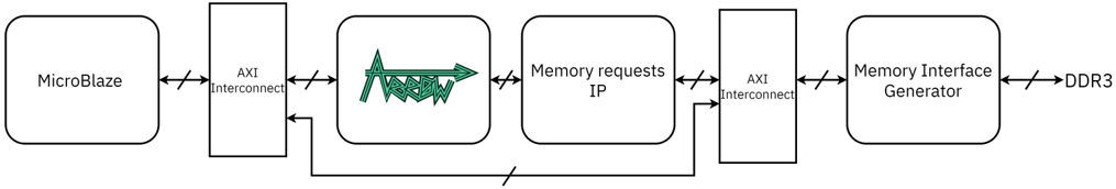
The image is a technical block diagram illustrating a digital system architecture, likely for an embedded or FPGA-based design. It depicts the data flow and interconnection between a processor core, bus interconnects, a memory controller, and external memory. The diagram is presented in a clean, schematic style with black outlines on a white background.
### Components/Axes
The diagram consists of six primary rectangular blocks and one external label, connected by directional arrows. The components are arranged horizontally from left to right, with a feedback loop at the bottom.
**Components (from left to right):**
1. **MicroBlaze**: A rectangular block on the far left. This is a soft processor core IP.
2. **AXI Interconnect**: A vertical rectangular block. This is the first of two identical components.
3. **AWEN**: A rectangular block containing a stylized green arrow pointing right, with the text "AWEN" integrated into the arrow's shaft. This likely represents an Address/Write Enable or similar control module.
4. **Memory requests IP**: A rectangular block.
5. **AXI Interconnect**: A second vertical rectangular block, identical to the first.
6. **Memory Interface Generator**: A rectangular block on the right.
7. **DDR3**: A text label on the far right, outside the final block, indicating the external memory type.
**Connections & Flow:**
* **Primary Data Path (Left to Right):**
* `MicroBlaze` ↔ `AXI Interconnect` (Bidirectional arrow with a slash, indicating a bus).
* `AXI Interconnect` ↔ `AWEN` (Bidirectional arrow with a slash).
* `AWEN` → `Memory requests IP` (Single-headed arrow pointing right, with a slash).
* `Memory requests IP` ↔ `AXI Interconnect` (Bidirectional arrow with a slash).
* `AXI Interconnect` ↔ `Memory Interface Generator` (Bidirectional arrow with a slash).
* `Memory Interface Generator` ↔ `DDR3` (Bidirectional arrow with a slash).
* **Feedback Path:**
* A line originates from the bottom of the second `AXI Interconnect`, travels left underneath the main blocks, and connects to the bottom of the first `AXI Interconnect`. This line also has a slash, indicating it is a bus or multi-signal path.
### Detailed Analysis
* **Text Transcription:** All text is in English. The transcribed labels are: "MicroBlaze", "AXI Interconnect" (appears twice), "AWEN", "Memory requests IP", "Memory Interface Generator", and "DDR3".
* **Spatial Grounding:** The legend (component labels) is embedded directly within each block. The feedback loop is positioned at the bottom of the diagram, connecting the two `AXI Interconnect` blocks. The `AWEN` block is centrally located between the first interconnect and the memory request logic.
* **Component Isolation:**
* **Header/Left Region:** Contains the processing element (`MicroBlaze`) and the first bus interconnect.
* **Main/Center Region:** Contains the core memory control logic (`AWEN`, `Memory requests IP`) and the second bus interconnect.
* **Footer/Bottom Region:** Contains the feedback path connecting the two interconnects.
* **Right Region:** Contains the memory physical interface (`Memory Interface Generator`) and the external memory (`DDR3`).
### Key Observations
1. **Symmetrical Interconnects:** The use of two identical `AXI Interconnect` blocks suggests a layered or segmented bus architecture, possibly separating processor-local traffic from memory controller traffic.
2. **AWEN Module:** The distinct green arrow within the `AWEN` block is the only color element in the diagram, highlighting its potential importance as a control or arbitration point.
3. **Feedback Loop:** The connection from the second interconnect back to the first is a critical feature, implying a flow control, acknowledgment, or snoop mechanism that allows the memory subsystem to communicate status back towards the processor.
4. **Standard Interfaces:** The consistent use of "AXI" (Advanced eXtensible Interface) indicates compliance with the AMBA bus standard, common in SoC designs. "Memory Interface Generator" is a common IP block name (e.g., in Xilinx tools) for creating DDR memory controllers.
### Interpretation
This diagram represents a standard memory subsystem architecture for a soft-core processor system on an FPGA. The **MicroBlaze** CPU initiates memory transactions. These are routed through a first **AXI Interconnect**, which likely acts as a central switch for the processor's local bus.
The **AWEN** block and **Memory requests IP** form the core memory controller logic. The AWEN module may handle address decoding and write-enable signaling, while the Memory requests IP manages the queueing, scheduling, and protocol translation of requests destined for the physical memory.
The second **AXI Interconnect** acts as a bridge between the memory controller logic and the **Memory Interface Generator**, which handles the low-level, timing-critical signals for the **DDR3** SDRAM chip.
The **feedback loop** is architecturally significant. It allows the memory subsystem (or the second interconnect) to signal backpressure or busy status to the first interconnect. This prevents the processor from overwhelming the memory controller with requests it cannot currently service, which is essential for system stability.
In essence, the diagram shows a pipelined and modular approach to connecting a processor to external memory, with clear separation between bus routing, request management, and physical interface generation. The design prioritizes standard interfaces (AXI) and modular IP blocks for flexibility and reusability.