## Diagram: MicroBlaze Memory Interface Architecture
### Overview
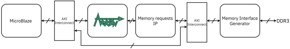
The diagram illustrates a data flow architecture connecting a MicroBlaze processor to a DDR3 memory module via intermediate components. The flow progresses through AXI Interconnects, a Memory requests IP block, and a Memory Interface Generator, with bidirectional communication paths indicated by bidirectional arrows.
### Components/Axes
1. **MicroBlaze**: Starting point of the data flow.
2. **AXI Interconnect**: Appears twice in the diagram:
- First instance connects MicroBlaze to the Memory requests IP block.
- Second instance connects the Memory requests IP block to the Memory Interface Generator.
3. **Memory requests IP**: Contains a green waveform symbol (likely representing AXI protocol signals).
4. **Memory Interface Generator**: Final processing block before DDR3.
5. **DDR3**: Endpoint representing the memory interface.
### Detailed Analysis
- **Flow Direction**:
- Data originates from MicroBlaze → AXI Interconnect → Memory requests IP (with AXI protocol signals) → AXI Interconnect → Memory Interface Generator → DDR3.
- **Bidirectional Communication**:
- All interconnects use bidirectional arrows (↔), indicating two-way data exchange.
- **Waveform Symbol**:
- The green waveform in the Memory requests IP block suggests AXI transaction signaling (e.g., address, data, control signals).
### Key Observations
- The architecture follows a layered design pattern common in embedded systems, separating processor logic (MicroBlaze) from memory interface logic (DDR3) via protocol translation blocks.
- The AXI Interconnect acts as a protocol translator between different IP blocks.
- The Memory requests IP block appears to handle request arbitration or protocol conversion for memory access.
### Interpretation
This diagram represents a typical embedded system memory subsystem architecture:
1. **MicroBlaze** generates memory requests using AXI protocol.
2. The **Memory requests IP** likely manages request queuing, arbitration, or protocol conversion to match the Memory Interface Generator's requirements.
3. The **Memory Interface Generator** translates these requests into DDR3-specific commands/timing.
4. The bidirectional AXI Interconnects suggest the system supports both read and write operations with full duplex communication.
The architecture demonstrates a modular design where:
- MicroBlaze operates independently of DDR3 specifics
- Protocol translation occurs at multiple stages (AXI Interconnects)
- Memory requests are processed through dedicated IP blocks before reaching the physical memory interface
This separation of concerns allows for:
- Easier IP block replacement/upgrades
- Protocol standardization (AXI)
- Timing optimization at each interface stage