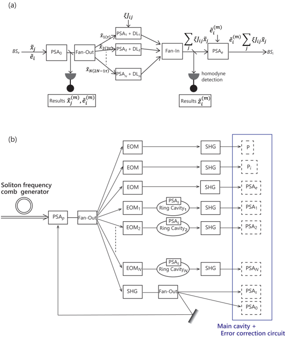
## Diagram: Optical Circuit Schematics
### Overview
The image presents two optical circuit schematics, labeled (a) and (b), detailing different configurations of optical components for signal processing and frequency comb generation. Both diagrams illustrate the flow of optical signals through various elements such as beam splitters, phase-sensitive amplifiers, electro-optic modulators, and second harmonic generators.
### Components/Axes
#### Diagram (a)
* **Input:** Beam splitter (BS<sub>e</sub>) with inputs x̄<sub>j</sub> and ē<sub>i</sub>
* **Components:**
* PSA<sub>0</sub> (Phase-Sensitive Amplifier)
* Fan-Out: Splits the signal into N paths.
* x̄<sub>1(τ)</sub>, x̄<sub>2(3τ)</sub>, ..., x̄<sub>N(2N-1τ)</sub>: Represent different signal paths after the Fan-Out.
* PSA<sub>1</sub> + DL<sub>1</sub>, PSA<sub>2</sub> + DL<sub>2</sub>, ..., PSA<sub>N</sub> + DL<sub>N</sub>: Phase-Sensitive Amplifiers with Delay Lines.
* Fan-In: Combines the signals from the N paths.
* ∑ξ<sub>ij</sub>ē<sub>i</sub><sup>(m)</sup>, ∑ξ<sub>ij</sub>x̄<sub>j</sub>: Represent the summed signals.
* PSA<sub>e</sub>: Phase-Sensitive Amplifier.
* Homodyne Detection: Measures the signal.
* **Output:** BS<sub>i</sub>
* **Results:** x̄<sub>j</sub><sup>(m)</sup>, ē<sub>i</sub><sup>(m)</sup> and z̄<sub>i</sub><sup>(m)</sup>
#### Diagram (b)
* **Input:** Soliton frequency comb generator.
* **Components:**
* PSA<sub>p</sub>: Phase-Sensitive Amplifier.
* Fan-Out: Splits the signal into multiple paths.
* EOM: Electro-Optic Modulators (multiple).
* EOM<sub>1</sub>, EOM<sub>2</sub>, ..., EOM<sub>N</sub>: Specific Electro-Optic Modulators.
* PSA<sub>s</sub> Ring Cavity<sub>1</sub>, PSA<sub>s</sub> Ring Cavity<sub>2</sub>, ..., PSA<sub>s</sub> Ring Cavity<sub>N</sub>: Phase-Sensitive Amplifiers within Ring Cavities.
* SHG: Second Harmonic Generators (multiple).
* Fan-Out: Splits the signal into multiple paths.
* **Output:**
* P, P<sub>i</sub>, PSA<sub>e</sub>, PSA<sub>1</sub>, PSA<sub>2</sub>, ..., PSA<sub>N</sub>, PSA<sub>s</sub>, PSA<sub>0</sub>: Represent different output signals.
* **Main cavity + Error correction circuit:** Encloses the output signals.
### Detailed Analysis or ### Content Details
#### Diagram (a)
The diagram illustrates a signal processing scheme. An input signal is split into multiple paths, each path undergoing phase-sensitive amplification and delay. These paths are then recombined and further amplified before being measured via homodyne detection.
* The input signal is split by the beam splitter (BS<sub>e</sub>) into two components, x̄<sub>j</sub> and ē<sub>i</sub>.
* The Fan-Out splits the signal into N paths.
* Each path has a PSA and a delay line (DL).
* The signals are recombined in the Fan-In.
* The output is measured using homodyne detection.
#### Diagram (b)
This diagram depicts a soliton frequency comb generator coupled with an error correction circuit. The comb generator's output is processed through a series of electro-optic modulators and second harmonic generators. Some paths include phase-sensitive amplifiers within ring cavities. The final outputs are fed into a main cavity and error correction circuit.
* The soliton frequency comb generator provides the initial signal.
* The signal is split by the Fan-Out.
* Multiple paths include EOMs and SHGs.
* Some paths include PSAs within ring cavities.
* The final outputs are fed into the "Main cavity + Error correction circuit".
### Key Observations
* Diagram (a) focuses on signal processing using phase-sensitive amplification and delay lines.
* Diagram (b) focuses on frequency comb generation and error correction.
* Both diagrams use Fan-Out and Fan-In components to split and combine signals.
* Diagram (b) includes ring cavities and second harmonic generation, which are not present in diagram (a).
### Interpretation
The diagrams illustrate two different optical circuit configurations. Diagram (a) likely represents a scheme for manipulating and measuring optical signals, while diagram (b) represents a more complex system for generating and stabilizing a frequency comb. The use of phase-sensitive amplifiers, delay lines, electro-optic modulators, and second harmonic generators suggests advanced techniques for controlling the phase, frequency, and amplitude of optical signals. The error correction circuit in diagram (b) indicates a focus on achieving high stability and precision in the frequency comb generation process.