## Circuit Diagrams: Feedback System and Op-Amp Equivalent Models
### Overview
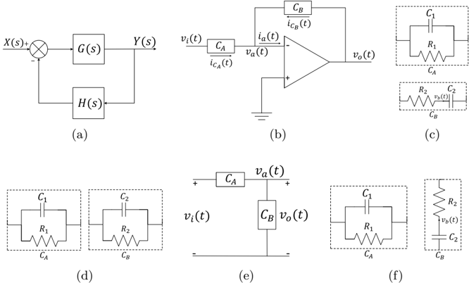
The image contains six distinct circuit diagrams labeled (a) through (f), presented in a 2x3 grid layout. These diagrams illustrate concepts from control theory and analog circuit design, specifically focusing on a feedback system and the equivalent circuit modeling of capacitors in an operational amplifier (op-amp) circuit.
### Components/Axes
The image is composed of six separate diagrams, each with its own set of labeled components and signals.
* **Diagram (a):** A classic negative feedback control system block diagram.
* **Signals:** Input `X(s)`, Output `Y(s)`.
* **Blocks:** Forward path transfer function `G(s)`, Feedback path transfer function `H(s)`.
* **Junction:** A summing junction where `X(s)` is added and the feedback signal is subtracted.
* **Diagram (b):** An inverting operational amplifier circuit.
* **Signals:** Input voltage `v_i(t)`, Output voltage `v_o(t)`, Node voltage `v_a(t)`, Currents `i_{C_A}(t)` and `i_{C_B}(t)`.
* **Components:** Two capacitors labeled `C_A` and `C_B`. The op-amp has its non-inverting terminal grounded.
* **Diagram (c):** Two separate equivalent circuit models, enclosed in dashed boxes.
* **Top Box (for `C_A`):** A parallel combination of a capacitor `C_1` and a resistor `R_1`.
* **Bottom Box (for `C_B`):** A series combination of a resistor `R_2`, a capacitor `C_2`, and a voltage source `v_{R_2}(t)`.
* **Diagram (d):** Two equivalent circuit models in dashed boxes, connected in series.
* **Left Box (for `C_A`):** Parallel combination of `C_1` and `R_1`.
* **Right Box (for `C_B`):** Parallel combination of `C_2` and `R_2`.
* **Diagram (e):** A simplified circuit model derived from diagram (b).
* **Signals:** Input `v_i(t)`, Output `v_o(t)`, Node voltage `v_a(t)`.
* **Components:** Two blocks labeled `C_A` and `C_B`, representing the equivalent impedances.
* **Diagram (f):** Two separate equivalent circuit models in dashed boxes.
* **Left Box (for `C_A`):** Parallel combination of `C_1` and `R_1`.
* **Right Box (for `C_B`):** Series combination of a resistor `R_2` and a capacitor `C_2`, with a voltage `v_{R_2}(t)` indicated across the resistor.
### Detailed Analysis
The diagrams progress from a general system concept to specific circuit implementations and their models.
1. **System-Level View (a):** This is a standard representation of a linear time-invariant (LTI) system with negative feedback. The closed-loop transfer function is `Y(s)/X(s) = G(s) / (1 + G(s)H(s))`.
2. **Circuit Implementation (b):** This shows a practical inverting amplifier where the input and feedback elements are generalized as impedances `Z_A` (labeled `C_A`) and `Z_B` (labeled `C_B`). The output is `v_o(t) = - (Z_B / Z_A) * v_i(t)`.
3. **Equivalent Circuit Models (c, d, f):** These diagrams propose different physical models for the capacitors `C_A` and `C_B`, likely to account for non-ideal characteristics like leakage resistance and series resistance.
* **Model (c):** `C_A` is modeled as a capacitor with parallel leakage (`C_1 || R_1`). `C_B` is modeled as a capacitor with series resistance and an associated voltage drop (`R_2` in series with `C_2`).
* **Model (d):** Both `C_A` and `C_B` are modeled simply as capacitors with parallel leakage resistance (`C_1 || R_1` and `C_2 || R_2`).
* **Model (f):** Similar to (c), but the电压源 `v_{R_2}(t)` is explicitly shown across the series resistor `R_2` for `C_B`. `C_A` remains a parallel RC model.
4. **Simplified Model (e):** This abstracts the circuit from (b) into a two-port network, focusing on the relationship between `v_i`, `v_o`, and the intermediate node `v_a` using the generalized impedances `C_A` and `C_B`.
### Key Observations
* The diagrams are interconnected. Diagram (b) is the physical circuit, (e) is its simplified schematic, and (c), (d), and (f) are different candidate models for the non-ideal capacitors within it.
* The labeling is consistent: `C_A` always refers to the input-side capacitor/impedance, and `C_B` always refers to the feedback-side capacitor/impedance.
* The models vary in complexity. Model (d) is the simplest (parallel RC for both). Models (c) and (f) are more complex, modeling the feedback capacitor `C_B` with a series RC network, which is a common model for real capacitors at higher frequencies.
* All diagrams use standard electrical engineering symbols for resistors, capacitors, op-amps, grounds, and signal sources.
### Interpretation
This set of diagrams serves as a technical exposition on modeling real-world components in circuit analysis. The progression demonstrates a fundamental engineering approach:
1. **Start with an ideal system model** (a: block diagram).
2. **Implement it with physical components** (b: op-amp circuit).
3. **Acknowledge component non-idealities** by creating more accurate equivalent circuits (c, d, f).
4. **Simplify the analysis** by using the equivalent impedance blocks (e).
The core message is that a capacitor in a circuit is not just an ideal `C`. Its behavior is better represented by models that include parasitic elements like parallel leakage resistance (`R_1` in models for `C_A`) and series resistance (`R_2` in models for `C_B`). The choice of model (parallel RC vs. series RC) depends on the frequency of operation and the specific characteristics of the capacitor being used. Diagram (f) explicitly highlighting `v_{R_2}(t)` suggests an analysis focus on the voltage drop across the parasitic series resistance, which becomes significant at high frequencies or with high ripple currents. This collection of figures would typically be used in a textbook or technical paper to explain the frequency response or stability analysis of active filters or integrator circuits built with real op-amps and capacitors.