## Block Diagram and Circuit Analysis
### Overview
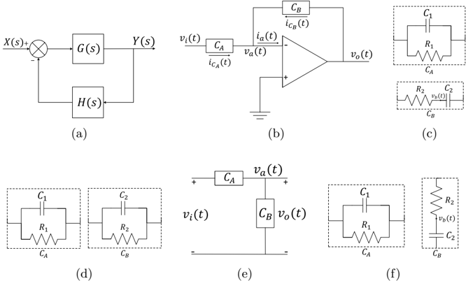
The image contains six technical diagrams (a-f) representing electronic systems and circuits. Diagrams (a) and (b) depict signal processing and operational amplifier configurations, while (c)-(f) illustrate impedance models and voltage divider circuits. All components are labeled with standard electrical symbols.
### Components/Axes
**Diagram (a): Block Diagram**
- Input: $ X(s) $ (positive and negative terminals)
- Transfer functions: $ G(s) $, $ H(s) $
- Output: $ Y(s) $
- Feedback loop: $ H(s) $ connects output to input via summing junction
**Diagram (b): Operational Amplifier Circuit**
- Components:
- $ C_A $, $ C_B $ (capacitors)
- $ i_{C_A}(t) $, $ i_{C_B}(t) $ (capacitor currents)
- $ v_i(t) $, $ v_a(t) $, $ v_o(t) $ (voltages)
- Configuration: Non-inverting amplifier with capacitive feedback
**Diagram (c): Impedance Models**
- Left: $ R_1 $ in parallel with $ C_1 $
- Right: $ R_2 $ in series with $ C_2 $
**Diagram (d): Parallel RC Circuits**
- Left: $ R_1 $ || $ C_1 $
- Right: $ R_2 $ || $ C_2 $
**Diagram (e): Capacitive Voltage Divider**
- Components: $ C_A $, $ C_B $ in series
- Voltages: $ v_i(t) $ (input), $ v_o(t) $ (output)
**Diagram (f): Combined Impedance Network**
- Left: $ R_1 $ || $ C_1 $
- Right: $ R_2 $ in series with $ C_2 $
### Detailed Analysis
**Diagram (a)** shows a feedback system with forward path $ G(s) $ and feedback path $ H(s) $. The summing junction combines $ X(s) $ and $ -H(s)Y(s) $.
**Diagram (b)** implements a non-inverting amplifier with capacitive feedback. The op-amp's negative input is connected to $ C_B $, while the positive input receives $ v_i(t) $ through $ C_A $.
**Diagrams (c)-(f)** represent different impedance configurations:
- (c): Series/parallel RC combinations
- (d): Pure parallel RC networks
- (e): Capacitive voltage divider
- (f): Mixed series-parallel RC network
### Key Observations
1. All diagrams use standard electrical symbols (resistors, capacitors, op-amps)
2. Time-domain signals ($ v(t) $) appear in (b) and (f), while (a) uses Laplace-domain transfer functions
3. Capacitors appear in all diagrams except (a)
4. Feedback appears in (a) and (b) but not in (c)-(f)
### Interpretation
These diagrams collectively demonstrate:
1. **Signal Processing**: Diagram (a) shows a basic feedback system with transfer functions
2. **Amplifier Design**: Diagram (b) implements a capacitive feedback amplifier
3. **Impedance Modeling**: Diagrams (c)-(f) show various RC network configurations for frequency response analysis
4. **Voltage Division**: Diagram (e) illustrates capacitive voltage division
The progression from block diagrams to physical circuits suggests a system design flow from mathematical modeling to implementation. The recurring use of capacitors indicates high-frequency applications or filtering requirements.