\n
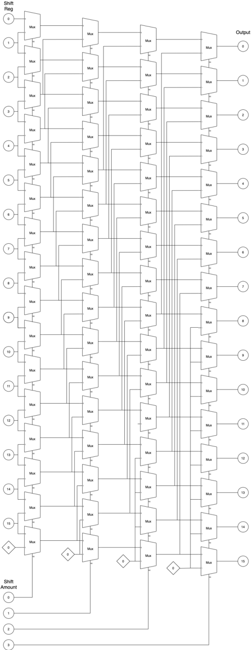
## Diagram: 16-bit Barrel Shifter Circuit
### Overview
The image is a detailed technical schematic of a 16-bit barrel shifter, a digital circuit used to shift a multi-bit data word by a specified number of bit positions in a single operation. The diagram is rendered in a clean, black-and-white line-art style. It depicts a network of 2-to-1 multiplexers (Mux) arranged in a regular grid, with inputs on the left, control signals at the bottom, and outputs on the right.
### Components/Axes
* **Primary Components:** The circuit is composed entirely of 2-to-1 multiplexer blocks, each labeled "Mux". There are 64 Mux blocks in total, arranged in 4 vertical columns of 16 Muxes each.
* **Inputs (Left Side):**
* A vertical column of 16 input lines, labeled **"Shift Reg"**.
* Each input is marked with a circled number from **0** (top) to **15** (bottom).
* **Outputs (Right Side):**
* A vertical column of 16 output lines, labeled **"Output"**.
* Each output is marked with a circled number from **0** (top) to **15** (bottom).
* **Control Inputs (Bottom):**
* A set of 4 control lines labeled **"Shift Amount"**.
* Each control line is marked with a circled number from **0** (left) to **3** (right). These represent the 4-bit binary value specifying the shift amount (0-15 positions).
* **Wiring & Connections:** A complex network of lines connects the inputs, Muxes, and outputs. The select (S) input of each Mux column is connected to one of the "Shift Amount" control lines.
* **Ground/Zero References:** Four diamond-shaped symbols containing the number **"0"** are present at the bottom of the diagram, connected to the '0' input of the first Mux in each column. This indicates that the least significant input for each stage is tied to a logical zero (ground).
### Detailed Analysis
**Circuit Function & Data Flow:**
This is a classic logarithmic barrel shifter architecture. The shift operation is broken down into stages, each controlled by one bit of the "Shift Amount" (SA).
1. **Stage 1 (Leftmost Column):** The select line for all Muxes in this column is connected to **SA[0]** (Shift Amount bit 0).
* If SA[0] = 0, each Mux passes its top input (which comes directly from the corresponding "Shift Reg" input or the previous stage's output) unchanged.
* If SA[0] = 1, each Mux selects its bottom input, which is wired to the bit one position lower (e.g., Mux for Output 5 gets input from Shift Reg 4). This stage shifts the data **1 bit** to the left (towards LSB) if enabled.
2. **Stage 2 (Second Column):** The select line is connected to **SA[1]**.
* If SA[1] = 1, this stage shifts the data **2 bit positions**. The wiring shows each Mux's bottom input is connected to the bit two positions lower in the previous stage's output.
3. **Stage 3 (Third Column):** The select line is connected to **SA[2]**.
* If SA[2] = 1, this stage shifts the data **4 bit positions**.
4. **Stage 4 (Rightmost Column):** The select line is connected to **SA[3]**.
* If SA[3] = 1, this stage shifts the data **8 bit positions**.
**Wiring Pattern (Example for Output 7):**
* **Output 7** is the output of the final Mux in the rightmost column.
* Its two inputs come from the corresponding Mux in the third column (for no 8-bit shift) and from the Mux for Output (7-8) = Output -1, which wraps to the bottom of the previous stage (Output 15 of the third column) for an 8-bit shift.
* Tracing back, the value at Output 7 is ultimately selected from one of the original "Shift Reg" inputs based on the binary combination of SA[3:0]. For example:
* SA = 0000 (0): Output 7 = Shift Reg 7.
* SA = 0001 (1): Output 7 = Shift Reg 8.
* SA = 0101 (5): Output 7 = Shift Reg 12 (7 + 5 = 12).
* SA = 1111 (15): Output 7 = Shift Reg 6 (7 + 15 = 22, modulo 16 = 6).
### Key Observations
1. **Regular, Scalable Structure:** The circuit is highly regular, composed of identical Mux blocks repeated in a grid. This makes it suitable for VLSI layout and scalable to different bit-widths.
2. **Binary-Weighted Stages:** The four columns correspond to the four bits of the shift amount, providing shifts of 1, 2, 4, and 8 positions. Any shift from 0 to 15 can be achieved by enabling the appropriate combination of stages (e.g., shift 7 = enable stages 1, 2, and 4).
3. **Single-Cycle Operation:** The combinational logic (no clocks or registers shown) implies the shift completes in one propagation delay, making it very fast.
4. **Zero-Padding:** The diamond "0" symbols indicate that bits shifted in from the "right" (the most significant side during a left shift) are filled with zeros. This is a logical left shift operation.
5. **Spatial Layout:** Inputs flow left-to-right. Control signals enter from the bottom and propagate vertically up each column. The legend (component labels) is integrated directly next to the components they describe.
### Interpretation
This diagram is a precise blueprint for a fundamental arithmetic logic unit (ALU) component. Its purpose is to perform **arbitrary, single-cycle bit shifts** on a 16-bit data word.
* **What it demonstrates:** It visually explains the principle of decomposing a complex shift operation (by N bits) into a series of simpler, binary-weighted shifts (by 1, 2, 4, 8 bits). This is a classic example of using logarithmic decomposition to achieve efficiency in hardware.
* **Relationships:** The "Shift Amount" is the master control. Its binary value directly determines which columns of Muxes are activated, which in turn determines the path each input bit takes through the network to become an output bit. The relationship is a direct mapping: `Output[i] = Input[(i + Shift_Amount) mod 16]`.
* **Notable Anomalies/Patterns:** There are no anomalies; the pattern is perfectly regular and deterministic. The most notable pattern is the "wrap-around" wiring for large shifts, where an output near the top (e.g., Output 0) gets its input for an 8-bit shift from an output near the bottom of the previous stage (Output 8), implementing the modulo-16 arithmetic.
* **Practical Significance:** This circuit is critical in processors for operations like multiplication/division by powers of two, bit masking, and aligning data. Its design prioritizes speed (single-cycle) over area (uses many Muxes), which is typical for high-performance computing. The diagram serves as an essential reference for hardware engineers to understand, verify, or implement this specific shifter design.