## Diagram: Comparison of Integrated Circuit (IC) Placement and Routing Layouts
### Overview
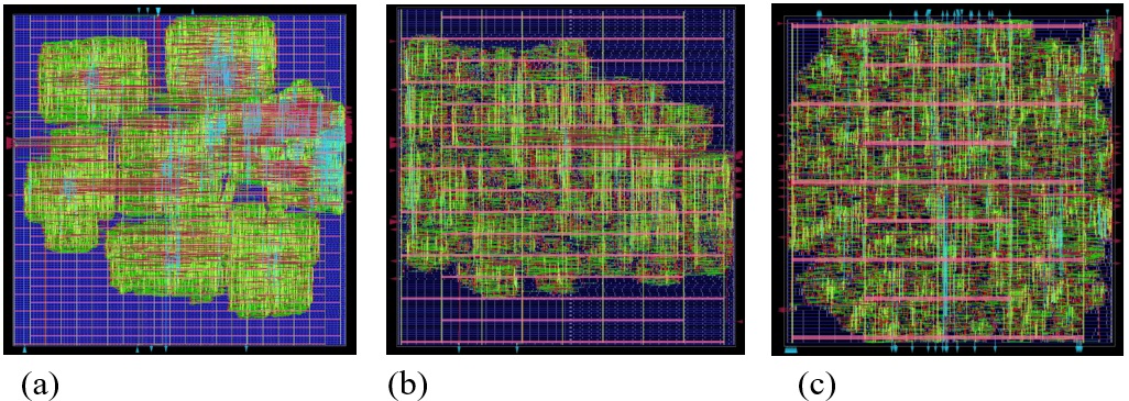
The image displays three distinct physical design layouts for an integrated circuit, labeled (a), (b), and (c). These diagrams represent different stages or methodologies in the VLSI (Very Large Scale Integration) design flow, specifically focusing on the placement of logic cells and the routing of interconnects on a silicon die.
### Components/Axes
* **Labels:** (a), (b), and (c) are positioned directly below their respective diagrams.
* **Visual Elements (Common to all):**
* **Green Blocks:** Represent standard cells or logic clusters.
* **Blue Grid:** Represents the underlying floorplan or placement grid.
* **Pink/Red Lines:** Represent power/ground rails or global routing tracks.
* **Cyan/Light Blue Lines:** Represent signal routing or specific net connections.
### Detailed Analysis
#### (a) Left: Clustered/Hierarchical Placement
* **Visual Trend:** The layout is characterized by distinct, separated "islands" of green logic blocks.
* **Spatial Distribution:** There is significant empty space (blue grid) between the clusters. The logic is not uniformly distributed across the die.
* **Routing:** Routing (cyan lines) is concentrated within the clusters, with fewer long-distance connections between the islands.
* **Observation:** This layout suggests a hierarchical design approach where functional modules are kept physically separate to manage complexity or timing constraints.
#### (b) Center: Flat/Standard Cell Placement
* **Visual Trend:** The logic (green blocks) is distributed much more uniformly across the entire area of the die compared to (a).
* **Spatial Distribution:** The density of the green blocks is high and relatively consistent. There is very little empty space.
* **Routing:** The cyan signal routing is more complex and spans the entire die, indicating a "flattened" design where hierarchy has been removed to optimize area utilization.
* **Observation:** This represents a standard cell placement where the goal is to maximize the utilization of the silicon area.
#### (c) Right: Structured/Routing-Optimized Layout
* **Visual Trend:** This layout is highly structured. It features prominent, evenly spaced horizontal pink lines (likely power/ground rails) running across the entire die.
* **Spatial Distribution:** The green logic blocks are packed tightly between the horizontal rails.
* **Routing:** The cyan routing is dense and appears to follow a more rigid, grid-like structure compared to (b).
* **Observation:** This represents a mature, optimized layout, likely post-routing, where power distribution networks (the pink lines) have been integrated, and signal routing is constrained by the physical grid.
### Key Observations
* **Density Progression:** There is a clear progression in density from (a) to (c). (a) is sparse/clustered, (b) is dense/flat, and (c) is highly structured/optimized.
* **Structural Evolution:** The diagrams illustrate the transition from a logical/hierarchical view (a) to a physical implementation view (c).
* **Routing Complexity:** The complexity of the interconnects (cyan lines) increases significantly from (a) to (c), reflecting the transition from initial placement to final routing.
### Interpretation
The data demonstrates the evolution of an integrated circuit design through the Electronic Design Automation (EDA) flow:
1. **Hierarchical Design (a):** This is likely an early stage of the physical design. By clustering logic, designers can manage timing and congestion for specific modules independently. The large whitespace suggests this is not yet optimized for area.
2. **Flattening (b):** This represents the "flattening" of the design. The hierarchy is removed, and the tool attempts to place all cells to minimize the total wire length and area. This is a standard step to improve performance and reduce die size.
3. **Physical Implementation (c):** This is the final stage. The inclusion of the horizontal pink lines indicates the addition of the Power/Ground (P/G) grid. The logic is now constrained by these rails, and the routing is finalized.
**Peircean Investigative Note:** The progression from (a) to (c) is not merely visual; it is a functional progression. If one were to attempt to manufacture (a), it would likely be inefficient in terms of silicon area. If one were to attempt to manufacture (b) without the power grid seen in (c), the chip would fail due to voltage drop (IR drop) issues. Therefore, these images serve as a visual timeline of the physical design process, moving from logical intent (a) to physical reality (c).