\n
## Diagram: Circuit Schematic
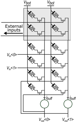
### Overview
The image depicts a circuit schematic, likely representing a buffer or driver circuit, constructed from multiple MOSFET transistors. The diagram shows a symmetrical arrangement of transistors, suggesting a balanced design. The schematic includes input voltages, output voltages, and a current source representation.
### Components/Axes
The diagram includes the following labeled components:
* **V<sub>bot</sub>**: Appears twice at the top of the schematic, connected to the gate of several transistors.
* **External inputs**: An arrow pointing into the circuit, indicating the location of external input signals.
* **V<sub>in</sub><0>**: Input voltage labeled as "V in less than 0".
* **V<sub>in</sub><1>**: Input voltage labeled as "V in less than 1".
* **V<sub>out</sub><0>**: Output voltage labeled as "V out less than 0".
* **V<sub>out</sub><1>**: Output voltage labeled as "V out less than 1".
* **i<sub>buff</sub>**: Current source labeled as "i buff", appearing twice at the bottom of the schematic.
The diagram consists of multiple MOSFET transistors arranged in a grid-like structure. Each transistor is represented by its standard schematic symbol. The transistors are connected in a way that suggests a differential amplifier or buffer configuration.
### Detailed Analysis / Content Details
The circuit consists of two main columns of transistors. Each column has a series of transistors connected between V<sub>bot</sub> and the output nodes V<sub>out</sub><0> and V<sub>out</sub><1> respectively.
* **Transistor Arrangement:** Each column contains six transistors. The top two transistors in each column are connected to V<sub>bot</sub>. The next two transistors are connected to V<sub>in</sub><0>, and the final two are connected to V<sub>in</sub><1>.
* **Output Connections:** The outputs of the transistors are connected to the current sources i<sub>buff</sub>, which in turn are connected to the output nodes V<sub>out</sub><0> and V<sub>out</sub><1>.
* **Symmetry:** The circuit is largely symmetrical, with identical arrangements of transistors in both columns. This suggests a balanced design intended to minimize common-mode noise and distortion.
* **Input Signal Path:** The "External inputs" arrow indicates that the input signals are applied to the transistors connected to V<sub>in</sub><0> and V<sub>in</sub><1>.
* **Transistor Type:** The transistors appear to be n-channel MOSFETs, based on their schematic symbols.
### Key Observations
* The symmetrical arrangement of transistors suggests a differential amplifier or buffer configuration.
* The use of current sources (i<sub>buff</sub>) indicates a desire for stable and predictable output current.
* The circuit appears to be designed to amplify or buffer input signals while maintaining a high degree of symmetry and stability.
* The labels V<sub>in</sub><0> and V<sub>in</sub><1> and V<sub>out</sub><0> and V<sub>out</sub><1> suggest that the circuit handles signals with a binary representation.
### Interpretation
This circuit schematic likely represents a buffer or driver stage in a digital or analog integrated circuit. The symmetrical design and use of current sources suggest a focus on high performance, stability, and noise immunity. The circuit is designed to take input signals (V<sub>in</sub><0> and V<sub>in</sub><1>) and produce corresponding output signals (V<sub>out</sub><0> and V<sub>out</sub><1>), potentially with amplification or impedance transformation. The "External inputs" arrow indicates that the circuit is intended to interface with external signals. The use of MOSFET transistors suggests that the circuit is designed for low-power operation and high switching speeds. The circuit could be part of a larger system, such as a data converter, a communication interface, or a memory circuit. The notation with the less than symbols (<0>, <1>) suggests these are bit-indexed signals.