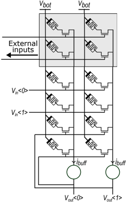
## Circuit Diagram: Dual-Input Voltage-Controlled Buffer Circuit
### Overview
The diagram illustrates a dual-input, dual-output buffer circuit with voltage-controlled switching elements. It features two input voltage sources (V_in<0> and V_in<1>), two output voltage nodes (V_out<0> and V_out<1>), and a matrix of voltage-controlled switches (V_bot) arranged in a 2x2 grid. Buffer currents (i_buff) are shown flowing from the output nodes.
### Components/Axes
- **Voltage-Controlled Switches (V_bot)**:
- Positioned at the top of the diagram, labeled "V_bot" on both sides.
- Represented by switch symbols with wavy lines, connected to input/output nodes.
- **Input Voltages**:
- Labeled "V_in<0>" and "V_in<1>", positioned vertically on the left side.
- Connected to the lower row of switches via vertical lines.
- **Output Voltages**:
- Labeled "V_out<0>" and "V_out<1>", positioned vertically at the bottom.
- Connected to the upper row of switches via vertical lines.
- **Buffer Currents (i_buff)**:
- Indicated by green arrows pointing downward from the output nodes.
- Labeled "i_buff" at the base of the output connections.
### Detailed Analysis
- **Switch Matrix Structure**:
- The 2x2 grid of switches connects input voltages (V_in<0>, V_in<1>) to output voltages (V_out<0>, V_out<1>).
- Each switch column is controlled by a shared V_bot voltage, suggesting multiplexing/demultiplexing functionality.
- **Signal Flow**:
- External inputs enter from the left, passing through switches to reach output nodes.
- V_bot controls switch states, determining which input voltage is routed to which output.
- **Symmetry**:
- Identical switch configurations on both sides of the diagram imply mirrored functionality for the two output channels.
### Key Observations
1. **No Numerical Values**: The diagram lacks explicit voltage/current values, focusing on structural relationships.
2. **Voltage Control**: V_bot acts as a control signal, modulating switch states to route inputs to outputs.
3. **Buffer Functionality**: The output nodes are labeled as buffers, suggesting isolation or amplification of input signals.
### Interpretation
This circuit likely functions as a **voltage-controlled routing network**, where V_bot determines signal paths between inputs and outputs. The dual-input, dual-output