## Multi-Panel Figure: Memristor Circuit and Characterization
### Overview
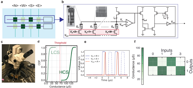
The image presents a multi-panel figure detailing a memristor-based circuit, its characterization, and performance. The figure includes a schematic diagram of the circuit, a photograph of the experimental setup, cumulative distribution functions (CDFs) of conductance, voltage waveforms, and a conductance heatmap.
### Components/Axes
**Panel a:**
* **Labels:** `<N>`, `<W>`, `<S>`, `<E>` are placed above a schematic of a memristor array.
* The array consists of two rows of memristors, some filled in dark green, some light green, and some white.
* The array is enclosed in a light blue box.
**Panel b:**
* **Labels:** V<sub>bot</sub>, V<sub>in</sub><0>, V<sub>in</sub><1>, V<sub>in</sub><N>, V<sub>top</sub>, V<sub>x</sub>, i<sub>in</sub>, i<sub>buff</sub>, i<sub>ref</sub>, V<sub>out</sub>, G<sub>0</sub>, G<sub>1</sub>, G<sub>N</sub>.
* The panel shows a circuit diagram with memristors connected to an amplifier and other circuit elements.
* Microscope images of the device are shown as insets.
**Panel c:**
* A photograph of the experimental setup, including a microscope and associated electronics.
**Panel d:**
* **Axes:**
* X-axis: Conductance (µS), ranging from 0 to 125.
* Y-axis: CDF, ranging from 0.0 to 1.0.
* **Labels:** "Threshold" (vertical dashed red line at approximately 60 µS), "LCS" (light green curve), "HCS" (dark green curve).
**Panel e:**
* **Axes:**
* X-axis: Time (µs), ranging from -4 to 8.
* Y-axis: Voltage (V), ranging from 0.0 to 1.2.
* **Labels:** V<sub>in</sub><N> (blue dashed line), V<sub>in</sub><S> (red dashed-dotted line), V<sub>out</sub><E> (solid black line).
**Panel f:**
* **Axes:**
* X-axis: Inputs, labeled 0, 1, 2, 3.
* Y-axis: Outputs, labeled 0, 1.
* Vertical Colorbar: Conductance (µS), ranging from 0 to 100.
* The panel shows a 2x4 heatmap with varying shades of green, representing conductance values.
### Detailed Analysis
**Panel d (CDF Plot):**
* **LCS (Light Green):** The CDF of the LCS (Low Conductance State) starts at 0 and rises sharply, reaching 1.0 around 50 µS.
* **HCS (Dark Green):** The CDF of the HCS (High Conductance State) starts at 0 and rises more gradually, reaching approximately 0.3 at 125 µS.
* **Threshold:** The vertical red dashed line indicates a threshold value of approximately 60 µS.
**Panel e (Voltage Waveforms):**
* **V<sub>in</sub><N> (Blue Dashed):** The input voltage at node N switches between approximately 0 V and 1.2 V.
* **V<sub>in</sub><S> (Red Dashed-Dotted):** The input voltage at node S switches between approximately 0 V and 1.2 V, with a slight delay compared to V<sub>in</sub><N>.
* **V<sub>out</sub><E> (Solid Black):** The output voltage at node E switches between approximately 0 V and 1.2 V, responding to the input voltages.
**Panel f (Conductance Heatmap):**
* The heatmap represents the conductance values for different input and output combinations.
* The conductance values range from approximately 20 µS (lightest green) to 80 µS (darkest green).
* Specific conductance values for each input/output combination:
* Output 0:
* Input 0: ~80 µS
* Input 1: ~20 µS
* Input 2: ~80 µS
* Input 3: ~20 µS
* Output 1:
* Input 0: ~20 µS
* Input 1: ~80 µS
* Input 2: ~20 µS
* Input 3: ~80 µS
### Key Observations
* The CDF plot (Panel d) shows a clear separation between the low and high conductance states of the memristor.
* The voltage waveforms (Panel e) demonstrate the switching behavior of the memristor circuit in response to input signals.
* The conductance heatmap (Panel f) indicates that the memristor array can perform logic operations based on the input signals.
### Interpretation
The data presented in the figure demonstrates the functionality of a memristor-based circuit. The CDF plot confirms the existence of distinct conductance states, which are essential for memristor-based memory and logic applications. The voltage waveforms show the dynamic response of the circuit to input signals, indicating its ability to perform switching operations. The conductance heatmap illustrates the potential of the memristor array for implementing logic functions, where different input combinations result in distinct output conductance values. The arrangement of the memristors and the circuit design enable the implementation of logic gates or other computational functions. The experimental setup photograph provides context for the physical implementation of the circuit.