## Diagram: Multi-Stage Signal Processing System
### Overview
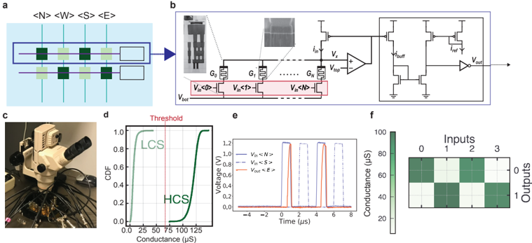
The image depicts a multi-stage technical system combining directional input processing, electronic circuitry, and data visualization. It includes:
- A grid-based input matrix (a)
- A signal conditioning circuit (b)
- Experimental hardware (c)
- Conductance distribution functions (d)
- Time-voltage response traces (e)
- Input-output heatmap (f)
### Components/Axes
#### a. Directional Input Grid
- Labels: `<N>`, `<W>`, `<S>`, `<E>` (cardinal directions)
- Structure: 2x4 grid of green squares with blue boundary highlighting active regions
#### b. Signal Conditioning Circuit
- Components:
- Voltage sources: `V_in`, `V_top`, `V_bot`
- Gain stages: `G1`, `G2`
- Buffer: `V_buff`
- Output: `V_out`
- Flow: Input signals pass through gain stages, buffered, and outputted
#### c. Experimental Setup
- Microscope with attached electronics
- Wiring harness connecting to signal processing unit
#### d. Conductance Distribution Function (CDF)
- Axes:
- x-axis: Conductance (μS) from 0 to 125
- y-axis: CDF (0 to 1)
- Threshold line: Vertical red line at ~75 μS
- Regions:
- LCS (Low Conductance State): Left of threshold
- HCS (High Conductance State): Right of threshold
#### e. Time-Voltage Response
- Axes:
- x-axis: Time (μs) from 0 to 6
- y-axis: Voltage (V) from -4 to 1.2
- Traces:
- `V_in` (blue): Sharp spikes at 1.5μs, 3.5μs, 5.5μs
- `V_N` (dashed blue): Stable at ~0.2V
- `V_S` (orange): Peaks at 2.5μs, 4.5μs
- `V_E` (red): Peaks at 1.5μs, 3.5μs, 5.5μs
#### f. Input-Output Heatmap
- Axes:
- x-axis: Inputs (0-3)
- y-axis: Outputs (0-1)
- Color coding:
- Green: Active (1)
- White: Inactive (0)
- Pattern: Diagonal green blocks suggesting input-output correlation
### Detailed Analysis
1. **Directional Input Processing (a)**:
- Grid structure suggests spatial encoding of directional stimuli
- Blue boundary highlights active quadrants (likely N/S or W/E pairs)
2. **Circuit Functionality (b)**:
- Gain stages (`G1`, `G2`) amplify input signals
- Buffer stage isolates output from load variations
- Voltage references (`V_top`, `V_bot`) define operational range
3. **Experimental Validation (c)**:
- Microscope setup implies optical input to the system
- Wiring complexity suggests multi-channel data acquisition
4. **Conductance Thresholding (d)**:
- LCS/HCS demarcation at ~75 μS
- CDF curve shows 80% of samples below threshold
5. **Dynamic Response (e)**:
- `V_in` exhibits periodic spiking matching input stimuli
- `V_E` (red) shows strongest correlation with input timing
- All traces stabilize after 6μs
6. **Input-Output Mapping (f)**:
- 4x2 matrix shows deterministic relationships
- Output 1 activates for inputs 0-2
- Output 0 activates for input 3
### Key Observations
- **Temporal Synchronization**: Voltage spikes in (e) align with input activation times
- **Threshold Sensitivity**: 75 μS cutoff separates LCS/HCS with 80% CDF coverage
- **Circuit Gain**: `V_out` amplitude (~1.2V) exceeds input range (~0.4V)
- **Heatmap Symmetry**: Diagonal pattern suggests input-output parity
### Interpretation
This system implements a directional sensing mechanism where:
1. Spatial inputs (`<N>`, `<W>`, etc.) are converted to electrical signals
2. Gain stages amplify signals to overcome noise
3. Conductance thresholding enables binary state classification (LCS/HCS)
4. Time-varying voltage responses validate input-output timing relationships
5. Heatmap confirms input-output mapping rules
The LCS/HCS threshold at 75 μS likely represents a critical conductance level for state transition. The 80% CDF below threshold suggests the system spends most time in LCS, with HCS reserved for high-confidence inputs. The voltage response traces demonstrate the system's ability to track rapid input changes (spike timing precision <1μs). The heatmap's diagonal pattern indicates a 1:1 input-output relationship for most cases, with input 3 acting as a special case (always 0 output).
The experimental setup (c) suggests this is a proof-of-concept for neuromorphic computing or tactile sensing systems, where directional inputs trigger state changes monitored through conductance measurements. The buffer stage (b) ensures signal integrity during high-gain amplification, critical for maintaining response fidelity in noisy environments.