## Circuit Diagram and State Machine: Memristor Array Control
### Overview
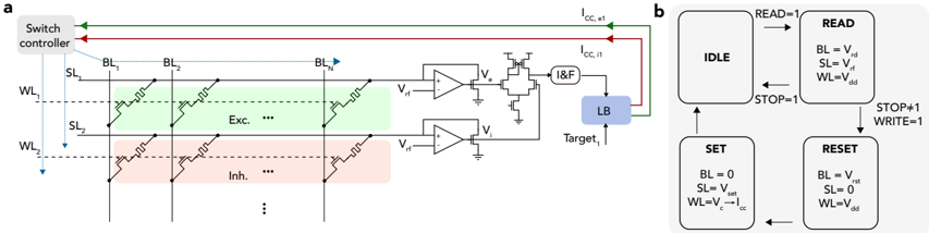
The image presents two diagrams. Diagram (a) depicts a circuit involving a memristor array connected to a switch controller and associated circuitry for reading and writing data. Diagram (b) shows a state machine outlining the operational states (IDLE, READ, SET, RESET) and transitions for controlling the memristor array.
### Components/Axes
**Diagram (a): Circuit Diagram**
* **Switch Controller:** Located at the top-left, connected to the memristor array via green and red lines.
* **Memristor Array:** A 2xN array of memristors.
* **Bit Lines (BL):** Labeled BL1, BL2, ..., BLN, running vertically.
* **Word Lines (WL):** Labeled WL1 and WL2, running horizontally.
* **Source Lines (SL):** Labeled SL1 and SL2, running horizontally.
* **Exc. (Excitation):** Green shaded region indicating excitatory memristors.
* **Inh. (Inhibition):** Red shaded region indicating inhibitory memristors.
* **Amplifiers:** Two amplifiers connected to the memristor array.
* Input voltages labeled as Vrf.
* Output voltages labeled as Ve and Vi.
* **I&F (Integrate and Fire):** A block receiving input from the amplifiers.
* **LB (Learning Block):** A blue block receiving input from the I&F block and outputting "Target1".
* **Current Lines:** Labeled Icc,e1 (green) and Icc,in (red), connecting the Learning Block back to the amplifier circuitry.
**Diagram (b): State Machine**
* **States:**
* IDLE: Initial state.
* READ: Reads data from the memristor array.
* SET: Sets the memristor to a specific state.
* RESET: Resets the memristor to a specific state.
* **Transitions:** Arrows indicate transitions between states, labeled with conditions (e.g., READ=1, STOP=1, WRITE=1).
* **State Parameters:** Each state includes values for Bit Line (BL), Source Line (SL), and Word Line (WL).
### Detailed Analysis
**Diagram (a): Circuit Diagram**
* The Switch Controller manages the activation of word lines (WL1, WL2) via blue arrows.
* The memristor array consists of memristors at the intersections of bit lines and word lines.
* The excitatory (Exc.) memristors are highlighted in green, while the inhibitory (Inh.) memristors are highlighted in red.
* The amplifiers compare the voltages from the memristor array (Vrf) and produce output voltages (Ve, Vi).
* The I&F block integrates the amplifier outputs and generates a signal for the Learning Block (LB).
* The Learning Block (LB) outputs a target signal (Target1) and provides feedback currents (Icc,e1, Icc,in) to the amplifier circuitry.
**Diagram (b): State Machine**
* **IDLE:**
* Transitions to READ state when READ=1.
* Transitions to SET state when STOP+1 and WRITE=1.
* **READ:**
* BL = Vrd
* SL = Vrf
* WL = Vdd
* Transitions to IDLE state when STOP=1.
* **SET:**
* BL = 0
* SL = Vset
* WL = Vc -> Icc
* Transitions to IDLE state.
* **RESET:**
* BL = Vrst
* SL = 0
* WL = Vdd
* Transitions to IDLE state.
### Key Observations
* The circuit diagram shows a memristor array with excitatory and inhibitory connections.
* The state machine defines the operational flow for reading, setting, and resetting the memristors.
* The state transitions are controlled by input signals (READ, STOP, WRITE).
* Each state has specific voltage levels applied to the bit lines, source lines, and word lines.
### Interpretation
The diagrams illustrate a system for controlling a memristor array, likely for neuromorphic computing or memory applications. The circuit diagram shows the physical connections and signal processing components, while the state machine defines the control logic for manipulating the memristor states. The use of excitatory and inhibitory memristors suggests a neural network implementation. The state machine ensures proper sequencing of operations for reading, writing, and resetting the memristors, enabling reliable data storage and processing. The feedback currents (Icc,e1, Icc,in) from the Learning Block to the amplifier circuitry suggest an adaptive learning mechanism.