## Diagram: Hardware Architecture for Parallel Processing System
### Overview
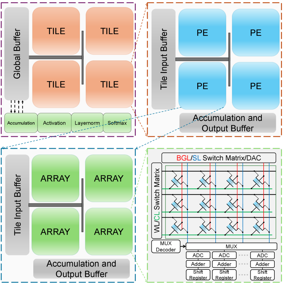
The diagram illustrates a multi-stage hardware architecture for parallel data processing, divided into four functional quadrants. It depicts data flow from input buffers through processing elements (PEs/ARRAYs) to output buffers, with specialized components for signal routing and analog/digital conversion.
### Components/Axes
1. **Top-Left Quadrant (Global Buffer)**
- **Global Buffer**: Central data reservoir
- **TILEs (4 units)**: Orange blocks labeled "TILE"
- **Processing Pipeline**:
- Accumulation (green)
- Activation (green)
- LayerNorm (green)
- Softmax (green)
2. **Top-Right Quadrant (Tile Input Buffer)**
- **Tile Input Buffer**: Gray vertical bar
- **PEs (4 units)**: Blue blocks labeled "PE"
- **Accumulation and Output Buffer**: Gray horizontal bar
3. **Bottom-Left Quadrant (Tile Input Buffer)**
- **Tile Input Buffer**: Gray vertical bar
- **ARRAYs (4 units)**: Green blocks labeled "ARRAY"
- **Accumulation and Output Buffer**: Gray horizontal bar
4. **Bottom-Right Quadrant (Signal Routing Matrix)**
- **BGL/SL Switch Matrix/DAC**:
- Red vertical lines (BGL)
- Blue vertical lines (SL)
- **WL/CL Switch Matrix**:
- Green horizontal lines
- **MUX Decoder**:
- 3-stage decoder with "MUX" labels
- **ADC/Adder/Shift Register Array**:
- 3 columns of ADC/Adder/Shift Register units
### Detailed Analysis
- **Data Flow Path**:
1. Global Buffer → TILEs/ARRAYs (parallel processing)
2. Tile Input Buffers → PEs/ARRAYs (local processing)
3. Accumulation Buffers → Output Buffer (final aggregation)
4. Switch Matrix → MUX Decoder → ADC/Adder/Shift Registers (signal conditioning)
- **Component Relationships**:
- TILEs and ARRAYs represent different processing paradigms (matrix vs. vector)
- PEs handle parallel computations with local accumulation
- Switch Matrix enables dynamic routing between processing units
- MUX Decoder manages multiplexing for efficient data distribution
- ADC/Adder/Shift Registers suggest analog signal processing capabilities
### Key Observations
1. **Dual Processing Paths**:
- TILEs (orange) and ARRAYs (green) suggest complementary processing capabilities
- PEs (blue) appear specialized for matrix operations
2. **Signal Conditioning Complexity**:
- 3-stage MUX Decoder indicates hierarchical multiplexing
- 9 ADC/Adder/Shift Register units suggest high-precision signal processing
3. **Buffer Hierarchy**:
- Global Buffer → Tile Input Buffers → Accumulation Buffers → Output Buffer
- Implies multi-level caching for performance optimization
### Interpretation
This architecture appears designed for high-performance neural network inference or scientific computing. The combination of TILEs (likely for matrix multiplications) and ARRAYs (for vector operations) enables efficient handling of different computational primitives. The PEs with local accumulation buffers suggest a systolic array architecture for parallel computation.
The bottom-right quadrant's complex routing matrix indicates support for dynamic computation graphs or adaptive processing paths. The presence of ADC/Adder/Shift Registers implies the system can handle mixed-signal processing, potentially for edge AI applications requiring sensor data fusion.
The buffer hierarchy demonstrates a thoughtful approach to data locality, minimizing latency by keeping intermediate results close to processing units. The switch matrix architecture enables flexible reconfiguration of data paths, allowing the system to adapt to different computational workloads without hardware changes.
Notably, the absence of explicit control logic in the diagram suggests these components interface with a separate control plane, likely managed by the MUX Decoder and associated logic. This separation of compute and control planes is common in modern accelerator architectures for improved scalability.