## ReRAM Array Analysis and Modeling
### Overview
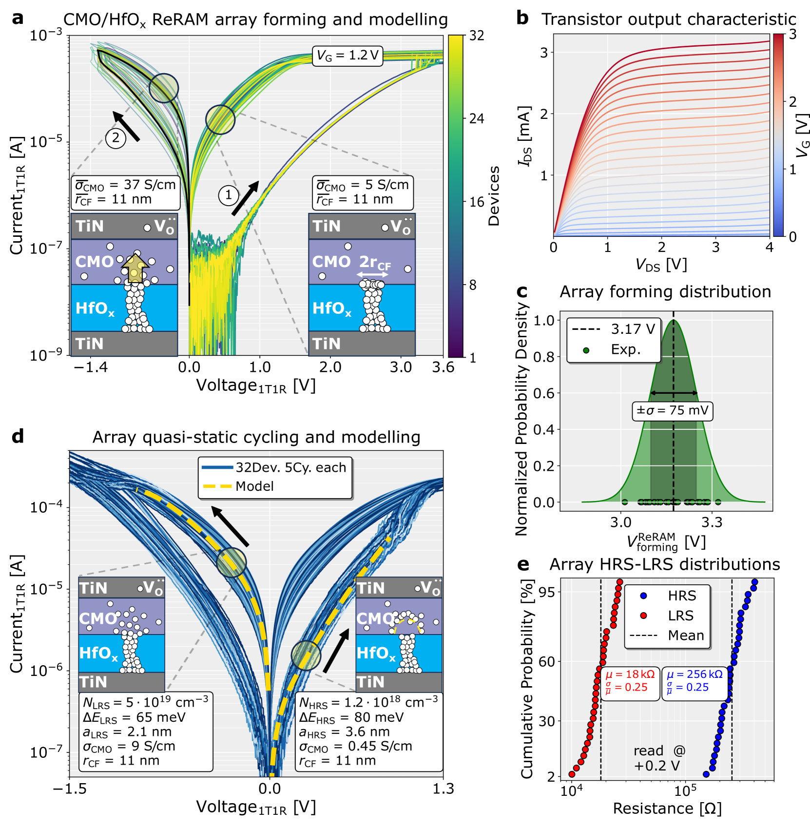
The image presents a comprehensive analysis of CMO/HfOx ReRAM (Resistive Random-Access Memory) array characteristics, transistor output, forming voltage distribution, quasi-static cycling behavior, and HRS/LRS (High Resistance State/Low Resistance State) distributions. It combines experimental data with modeling to provide insights into the device's performance and reliability.
### Components/Axes
**Figure a: CMO/HfOx ReRAM array forming and modelling**
* **Title:** CMO/HfOx ReRAM array forming and modelling
* **Y-axis:** Current$_{1T1R}$ [A], logarithmic scale from 10$^{-9}$ to 10$^{-3}$
* **X-axis:** Voltage$_{1T1R}$ [V], linear scale from -1.4 to 3.6
* **Colorbar:** Represents "Devices" ranging from 1 to 32. The color transitions from dark blue (1) to yellow (approximately 16) to bright yellow (32).
* **Annotations:**
* V$_G$ = 1.2 V
* Two diagrams showing the ReRAM structure with TiN/CMO/HfOx/TiN layers.
* Left diagram: Shows oxygen vacancies (V$_O$) moving upwards through the CMO layer. σ̄$_{CMO}$ = 37 S/cm, r$_{CF}$ = 11 nm.
* Right diagram: Shows a conductive filament (2r$_{CF}$) formed by oxygen vacancies in the HfOx layer. σ̄$_{CMO}$ = 5 S/cm, r$_{CF}$ = 11 nm.
* Arrows indicating the direction of current flow during forming (1) and reset (2).
**Figure b: Transistor output characteristic**
* **Title:** Transistor output characteristic
* **Y-axis:** I$_{DS}$ [mA], linear scale from 0 to 3
* **X-axis:** V$_{DS}$ [V], linear scale from 0 to 4
* **Colorbar:** Represents V$_G$ [V] ranging from 0 (blue) to 3 (red).
**Figure c: Array forming distribution**
* **Title:** Array forming distribution
* **Y-axis:** Normalized Probability Density, linear scale from 0.0 to 1.0
* **X-axis:** V$_{forming}^{ReRAM}$ [V], linear scale from 3.0 to 3.3
* **Legend:**
* Green dots: Exp. (Experimental data)
* Black dashed line: 3.17 V
* **Annotation:** ±σ = 75 mV
**Figure d: Array quasi-static cycling and modelling**
* **Title:** Array quasi-static cycling and modelling
* **Y-axis:** Current$_{1T1R}$ [A], logarithmic scale from 10$^{-7}$ to 10$^{-4}$
* **X-axis:** Voltage$_{1T1R}$ [V], linear scale from -1.5 to 1.3
* **Legend:**
* Blue lines: 32 Dev. 5 Cy. each (32 devices, 5 cycles each)
* Yellow dashed line: Model
* **Annotations:**
* Two diagrams showing the ReRAM structure with TiN/CMO/HfOx/TiN layers.
* Left diagram: Shows oxygen vacancies (V$_O$) moving upwards through the CMO layer. N$_{LRS}$ = 5 * 10$^{19}$ cm$^{-3}$, ΔE$_{LRS}$ = 65 meV, a$_{LRS}$ = 2.1 nm, σ$_{CMO}$ = 9 S/cm, r$_{CF}$ = 11 nm.
* Right diagram: Shows a conductive filament formed by oxygen vacancies in the HfOx layer. N$_{HRS}$ = 1.2 * 10$^{18}$ cm$^{-3}$, ΔE$_{HRS}$ = 80 meV, a$_{HRS}$ = 3.6 nm, σ$_{CMO}$ = 0.45 S/cm, r$_{CF}$ = 11 nm.
* Arrow indicating the direction of the cycling.
**Figure e: Array HRS-LRS distributions**
* **Title:** Array HRS-LRS distributions
* **Y-axis:** Cumulative Probability [%], linear scale from 2 to 95
* **X-axis:** Resistance [Ω], logarithmic scale from 10$^4$ to 10$^5$
* **Legend:**
* Blue dots: HRS (High Resistance State)
* Red dots: LRS (Low Resistance State)
* Black dashed line: Mean
* **Annotations:**
* μ = 18 kΩ, σ = 0.25 (for LRS)
* μ = 256 kΩ, σ = 0.25 (for HRS)
* read @ +0.2 V
### Detailed Analysis
**Figure a:**
* The current-voltage characteristics show the forming process of the ReRAM device. The current increases sharply at a certain voltage (forming voltage). The color gradient indicates the number of devices exhibiting similar behavior.
* The current increases with voltage for positive voltages.
* The current decreases with voltage for negative voltages.
**Figure b:**
* The transistor output characteristics show the relationship between drain current (I$_{DS}$) and drain-source voltage (V$_{DS}$) for different gate voltages (V$_G$). The drain current increases with both V$_{DS}$ and V$_G$, eventually saturating.
* The curves show saturation behavior, where the current plateaus at higher V$_{DS}$ values.
**Figure c:**
* The array forming distribution shows the distribution of forming voltages. The experimental data (green dots) is fitted with a Gaussian distribution. The mean forming voltage is 3.17 V, with a standard deviation of 75 mV.
* The distribution is approximately Gaussian.
**Figure d:**
* The quasi-static cycling curves show the switching behavior of the ReRAM device. The current-voltage characteristics exhibit hysteresis, indicating the switching between HRS and LRS. The model (yellow dashed line) captures the general trend of the experimental data (blue lines).
* The curves show hysteresis, indicating the switching behavior.
**Figure e:**
* The HRS-LRS distributions show the cumulative probability of resistance values in the high and low resistance states. The LRS distribution is centered around 18 kΩ, while the HRS distribution is centered around 256 kΩ.
* The LRS distribution is shifted to lower resistance values compared to the HRS distribution.
### Key Observations
* The ReRAM device exhibits clear forming and switching behavior.
* The transistor characteristics show typical saturation behavior.
* The forming voltage is narrowly distributed around 3.17 V.
* The HRS and LRS distributions are well-separated, indicating good switching characteristics.
### Interpretation
The data presented provides a comprehensive characterization of the CMO/HfOx ReRAM device. The forming process, transistor characteristics, switching behavior, and resistance distributions are all well-defined. The modeling results are in good agreement with the experimental data, suggesting that the model captures the essential physics of the device. The well-separated HRS and LRS distributions indicate that the device has good switching characteristics and is suitable for memory applications. The narrow distribution of forming voltages suggests good uniformity across the array. The diagrams showing the oxygen vacancy movement and conductive filament formation provide insights into the underlying switching mechanism.