## Chart/Diagram Type: ReRAM Device Characteristics & Modeling
### Overview
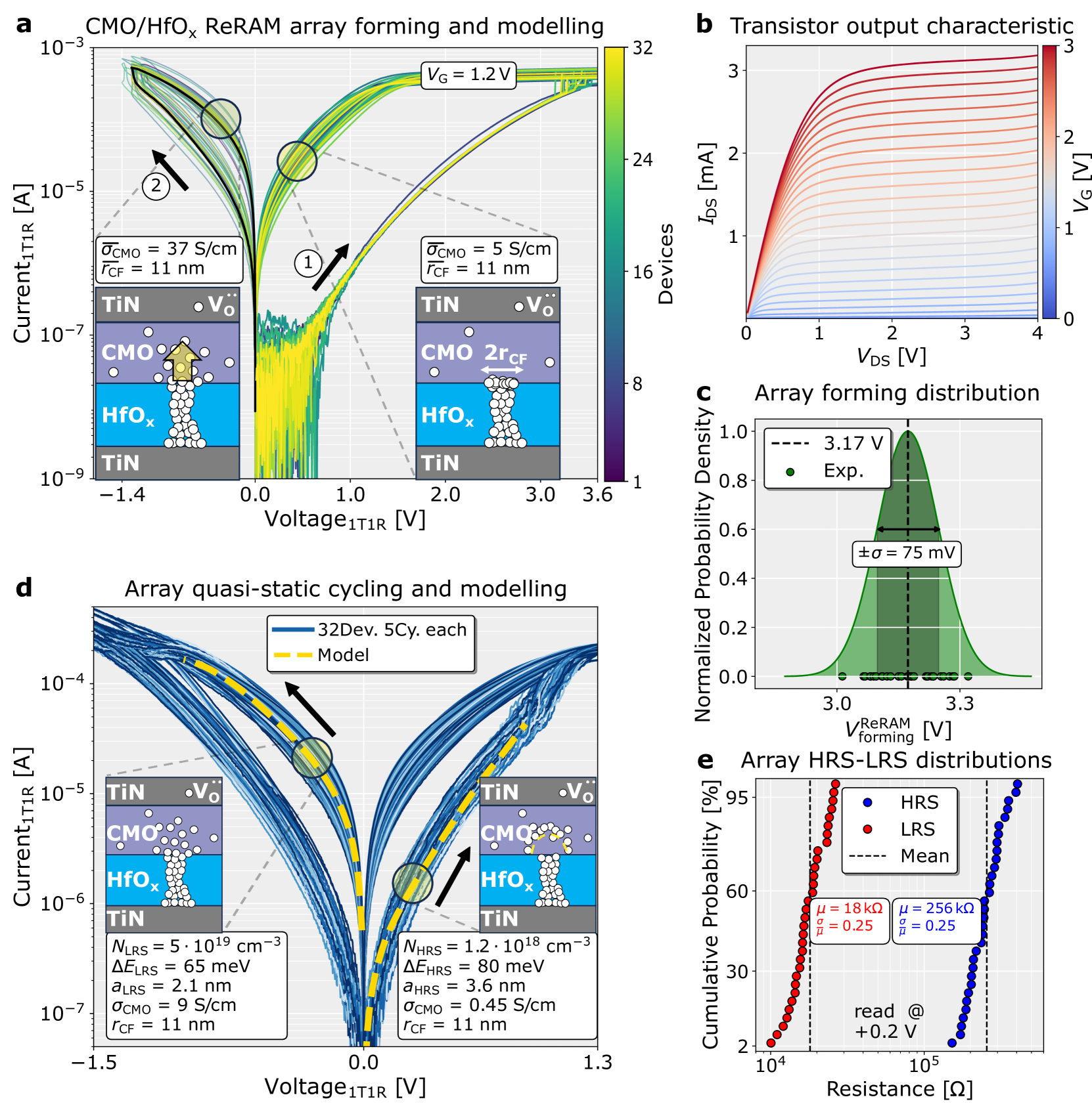
This image presents a series of charts and diagrams detailing the formation, modeling, and characteristics of a ReRAM (Resistive Random Access Memory) device based on a CMO/HfOx/TiN stack. It includes current-voltage characteristics during array forming, transistor output characteristics, array forming distribution, quasi-static cycling behavior, and high/low resistance state (HRS/LRS) distributions.
### Components/Axes
* **a) CMO/HfOx ReRAM array forming and modeling:**
* X-axis: Voltage<sub>1T1R</sub> [V] (ranging from -1.4 to 3.6 V)
* Y-axis: Current<sub>1T1R</sub> [A] (logarithmic scale, from 10<sup>-9</sup> to 10<sup>-3</sup> A)
* Color scale: Devices (ranging from 1 to 32)
* Labels: σ<sub>CMO</sub> = 37 S/cm, t<sub>CF</sub> = 11 nm (associated with device 1), σ<sub>CMO</sub> = 5 S/cm, t<sub>CF</sub> = 11 nm (associated with device 2), V<sub>G</sub> = 1.2V
* **b) Transistor output characteristic:**
* X-axis: V<sub>DS</sub> [V] (ranging from 0 to 4 V)
* Y-axis: I<sub>DS</sub> [mA] (left) and V<sub>G</sub> [V] (right, ranging from 0 to 3 V)
* **c) Array forming distribution:**
* X-axis: V<sub>ReRAM forming</sub> [V] (ranging from 3.0 to 3.3 V)
* Y-axis: Normalized Probability (ranging from 0 to 1.0)
* Error bar: ±σ = 75 mV
* **d) Array quasi-static cycling and modeling:**
* X-axis: Voltage<sub>1T1R</sub> [V] (ranging from -1.5 to 1.3 V)
* Y-axis: Current<sub>1T1R</sub> [A] (logarithmic scale, from 10<sup>-7</sup> to 10<sup>-4</sup> A)
* Lines: Model (orange), 32 cycles (blue)
* Labels: N<sub>LRS</sub> = 5 x 10<sup>19</sup> cm<sup>-3</sup>, ΔE<sub>LRS</sub> = 65 meV, δ<sub>LRS</sub> = 2.1 nm, σ<sub>CMO</sub> = 9 S/cm, t<sub>CF</sub> = 11 nm, N<sub>HRS</sub> = 1.2 x 10<sup>18</sup> cm<sup>-3</sup>, ΔE<sub>HRS</sub> = 80 meV, δ<sub>HRS</sub> = 3.6 nm, σ<sub>CMO</sub> = 0.45 S/cm, t<sub>CF</sub> = 11 nm
* **e) Array HRS-LRS distributions:**
* X-axis: Resistance [Ω] (logarithmic scale, from 10<sup>4</sup> to 10<sup>6</sup> Ω)
* Y-axis: Cumulative Probability [%] (ranging from 0 to 100%)
* Lines: HRS (red), LRS (blue), Mean (green)
* Labels: μ = 18 kΩ, σ = 0.25, μ = 256 kΩ, σ = 0.25, read @ +0.2 V
### Detailed Analysis or Content Details
* **a) CMO/HfOx ReRAM array forming and modeling:** The plot shows multiple current-voltage curves for different devices during the forming process. Device 1 (σ<sub>CMO</sub> = 37 S/cm, t<sub>CF</sub> = 11 nm) exhibits a sharp increase in current around 2.5V. Device 2 (σ<sub>CMO</sub> = 5 S/cm, t<sub>CF</sub> = 11 nm) shows a similar, but less pronounced, increase in current around 2.8V. The color gradient indicates the variation in forming voltage across the array.
* **b) Transistor output characteristic:** This is a standard transistor characteristic curve showing I<sub>DS</sub> as a function of V<sub>DS</sub> for different gate voltages V<sub>G</sub>. The curve shows a typical saturation region for the transistor.
* **c) Array forming distribution:** The distribution of forming voltages is centered around approximately 3.17 V, with a standard deviation of 75 mV. The experimental data (black dots) is relatively tightly distributed.
* **d) Array quasi-static cycling and modeling:** The plot shows the current-voltage behavior of the ReRAM device during repeated switching cycles (32 cycles). The modeled behavior (orange line) closely matches the experimental data (blue line). The device exhibits hysteresis.
* **e) Array HRS-LRS distributions:** The cumulative probability distributions for the high resistance state (HRS) and low resistance state (LRS) are shown. The HRS distribution is centered around 18 kΩ with a standard deviation of 0.25. The LRS distribution is centered around 256 kΩ with a standard deviation of 0.25. The read voltage is specified as +0.2 V.
### Key Observations
* The forming voltage varies across the ReRAM array, as indicated by the color gradient in (a).
* The modeled behavior in (d) closely matches the experimental data, suggesting the model accurately captures the device's switching characteristics.
* There is a significant difference in resistance between the HRS and LRS, enabling clear distinction between the two states.
* The distributions in (e) are relatively narrow, indicating good uniformity in the device's resistance states.
### Interpretation
The data demonstrates the successful fabrication and modeling of a CMO/HfOx/TiN ReRAM device. The array forming process exhibits some variation in forming voltage, which could be attributed to variations in the CMO layer or the HfOx film. The quasi-static cycling data confirms the device's ability to switch between HRS and LRS repeatedly. The narrow resistance distributions suggest good device uniformity, which is crucial for reliable memory operation. The model accurately predicts the device's behavior, providing a valuable tool for optimizing device design and performance. The read voltage of +0.2V is likely chosen to maximize the margin between the HRS and LRS, ensuring accurate data reading. The parameters like σ<sub>CMO</sub> and t<sub>CF</sub> are critical in determining the device's performance, and their values are provided for different devices to highlight the impact of material properties on the forming process.