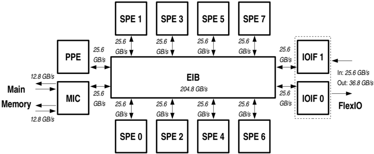
## Block Diagram: Cell Broadband Engine Architecture
### Overview
This image is a technical block diagram illustrating the high-level architecture and data pathways of the Cell Broadband Engine processor. It shows the central interconnect, processing elements, memory interface, and I/O interfaces, with specific data transfer rates labeled for each connection.
### Components/Axes
The diagram is organized around a central rectangular block labeled **EIB** (Element Interconnect Bus). Surrounding this central bus are several other functional blocks connected via bidirectional arrows.
**Central Component:**
* **EIB**: Labeled with a peak bandwidth of **204.8 GB/s**.
**Processing Elements (Top and Bottom Rows):**
* **SPE 1, SPE 3, SPE 5, SPE 7**: Located in a row above the EIB.
* **SPE 0, SPE 2, SPE 4, SPE 6**: Located in a row below the EIB.
* Each of these eight **SPE** (Synergistic Processing Element) blocks connects to the EIB with a labeled bandwidth of **25.6 GB/s**.
**Control and Memory Interface (Left Side):**
* **PPE** (Power Processing Element): Positioned to the left of the EIB, connected with a bandwidth of **25.6 GB/s**.
* **MIC** (Memory Interface Controller): Positioned below the PPE and to the left of the EIB. It connects to the EIB with a bandwidth of **25.6 GB/s**.
* **Main Memory**: Represented by text and arrows to the left of the MIC. The connection between Main Memory and the MIC is labeled with a bandwidth of **12.8 GB/s** (in both directions).
**I/O Interfaces (Right Side):**
* **IOIF 1** and **IOIF 0**: Two blocks enclosed within a dashed rectangle on the right side of the EIB.
* Each **IOIF** connects to the EIB with a bandwidth of **25.6 GB/s**.
* **IOIF 1** has an external input arrow labeled **In: 25.6 GB/s**.
* **IOIF 0** has an external output arrow labeled **Out: 36.8 GB/s** and is also connected to a label **FlexIO**.
### Detailed Analysis
**Spatial Layout and Connections:**
* The **EIB** is the central hub, with all other components connected directly to it.
* The eight **SPEs** are symmetrically placed, four above and four below the EIB.
* The **PPE** and **MIC** are stacked vertically on the left, forming the control and memory subsystem.
* The **IOIF** blocks are stacked vertically on the right, forming the I/O subsystem, with the dashed box suggesting they are part of a unified I/O interface group.
**Data Flow and Bandwidths:**
* **Internal Peak Bandwidth:** The EIB itself is rated for **204.8 GB/s**.
* **Component-to-EIB Links:** All direct connections from the EIB to the PPE, MIC, SPEs, and IOIFs are rated at **25.6 GB/s** each.
* **External Memory Link:** The path from the MIC to Main Memory has a lower bandwidth of **12.8 GB/s**.
* **External I/O Links:** The diagram specifies asymmetric external I/O bandwidths: **25.6 GB/s** for input (to IOIF 1) and **36.8 GB/s** for output (from IOIF 0).
### Key Observations
1. **Symmetry and Scalability:** The uniform connection bandwidth (25.6 GB/s) for all processing elements (SPEs) and the PPE to the EIB suggests a balanced, scalable design for parallel processing.
2. **Bandwidth Hierarchy:** There is a clear hierarchy: the internal EIB bandwidth (204.8 GB/s) is significantly higher than any single component link (25.6 GB/s), which in turn is higher than the main memory link (12.8 GB/s). This indicates a design optimized for high internal data movement.
3. **I/O Asymmetry:** The specified output bandwidth (36.8 GB/s) is higher than the input bandwidth (25.6 GB/s), which may reflect a design bias towards data processing and output (e.g., for graphics or scientific computation results).
4. **Component Roles:** The diagram clearly segregates functions: computation (SPEs, PPE), memory control (MIC), interconnection (EIB), and I/O (IOIFs).
### Interpretation
This diagram depicts a high-performance, heterogeneous multi-core processor architecture, specifically the Cell Broadband Engine used in systems like the PlayStation 3 and some supercomputers.
* **Architectural Philosophy:** The design emphasizes high-bandwidth, low-latency communication between specialized processing units via a central, high-speed bus (EIB). The PPE handles general-purpose control, while the eight SPEs are designed for intensive, parallel numerical computations.
* **Performance Implications:** The bottleneck for overall system performance is likely not the internal interconnect (EIB) but the external links, particularly the **12.8 GB/s** connection to main memory. This is a classic "memory wall" scenario where processor capability outpaces memory bandwidth.
* **Data Flow Inference:** The architecture is built for a "streaming" data model. Data flows in from I/O (e.g., 25.6 GB/s), is processed in parallel by the SPEs using data staged in their local stores (not shown), and results are streamed out (e.g., at 36.8 GB/s). The high EIB bandwidth facilitates the rapid shuffling of data between these units.
* **Design Intent:** The explicit labeling of bandwidths underscores that this architecture is engineered for predictable, high-throughput data processing, making it suitable for media processing, scientific simulation, and other bandwidth-intensive workloads. The asymmetry in I/O suggests it's optimized for workloads that generate more output data than input, or where output latency is critical.