\n
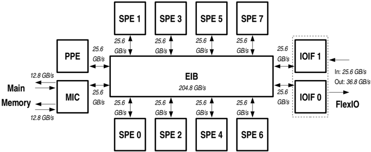
## Diagram: Cell Broadband Engine Architecture
### Overview
The image depicts the architecture of a Cell Broadband Engine (CBE), illustrating the interconnection of its core components: Main Memory, Memory Interface Controller (MIC), Power Processing Element (PPE), Element Interconnect Bus (EIB), Synergistic Processing Elements (SPEs), and Input/Output Interface (IOIF). The diagram focuses on data transfer rates between these components.
### Components/Axes
The diagram consists of the following components:
* **Main Memory:** Located on the left side of the diagram.
* **MIC (Memory Interface Controller):** Connected to Main Memory.
* **PPE (Power Processing Element):** Connected to both MIC and EIB.
* **EIB (Element Interconnect Bus):** The central interconnect, connecting PPE, MIC, and all SPEs and IOIFs.
* **SPE 0-7 (Synergistic Processing Elements):** Eight SPEs arranged in two rows, connected to the EIB.
* **IOIF 0 & 1 (Input/Output Interface):** Located on the right side of the diagram, connected to the EIB.
* **FlexIO:** Connected to IOIFs.
Data transfer rates are indicated along the arrows connecting the components, measured in GB/s (Gigabytes per second).
### Detailed Analysis
* **Main Memory <-> MIC:** 12.8 GB/s in both directions.
* **MIC <-> PPE:** 25.6 GB/s.
* **MIC <-> EIB:** 25.6 GB/s.
* **PPE <-> EIB:** 25.6 GB/s.
* **EIB <-> SPE 0-7:** Each SPE has a 25.6 GB/s connection to the EIB.
* **EIB <-> IOIF 0:** 25.6 GB/s.
* **EIB <-> IOIF 1:** 25.6 GB/s.
* **IOIF 1 Input (In):** 25.6 GB/s.
* **IOIF 1 Output (Out):** 36.8 GB/s.
* **EIB Bandwidth:** The EIB has a total bandwidth of 204.8 GB/s.
The SPEs are numbered 0 through 7, arranged in two rows of four. SPE 0, 2, 4, and 6 are in the bottom row, while SPE 1, 3, 5, and 7 are in the top row. All SPEs have equal bandwidth connections to the EIB. The IOIFs are depicted with dashed borders, suggesting they are external interfaces.
### Key Observations
* The EIB serves as the central high-bandwidth interconnect for all components.
* The SPEs have a consistent and relatively high bandwidth connection to the EIB.
* The Main Memory connection to the rest of the system is the narrowest bandwidth link at 12.8 GB/s.
* IOIF 1 has a higher output bandwidth (36.8 GB/s) than input bandwidth (25.6 GB/s).
### Interpretation
This diagram illustrates the CBE's heterogeneous architecture, designed for high-performance computing. The PPE acts as the control processor, while the SPEs are specialized processing units optimized for data-parallel tasks. The EIB provides a high-bandwidth pathway for communication between these elements. The relatively low bandwidth of the Main Memory connection suggests that the CBE is designed to minimize reliance on external memory access, favoring on-chip data processing and communication via the EIB. The asymmetric bandwidth of IOIF 1 suggests it is optimized for output-intensive operations. The overall architecture emphasizes parallel processing and efficient data transfer, making it suitable for applications like gaming, scientific simulations, and media processing. The diagram highlights the importance of the EIB as the central nervous system of the CBE, enabling rapid communication between the processing elements.