## PCB Layout: SynSense XYLO-AUDIO-V2 Daughter Board
### Overview
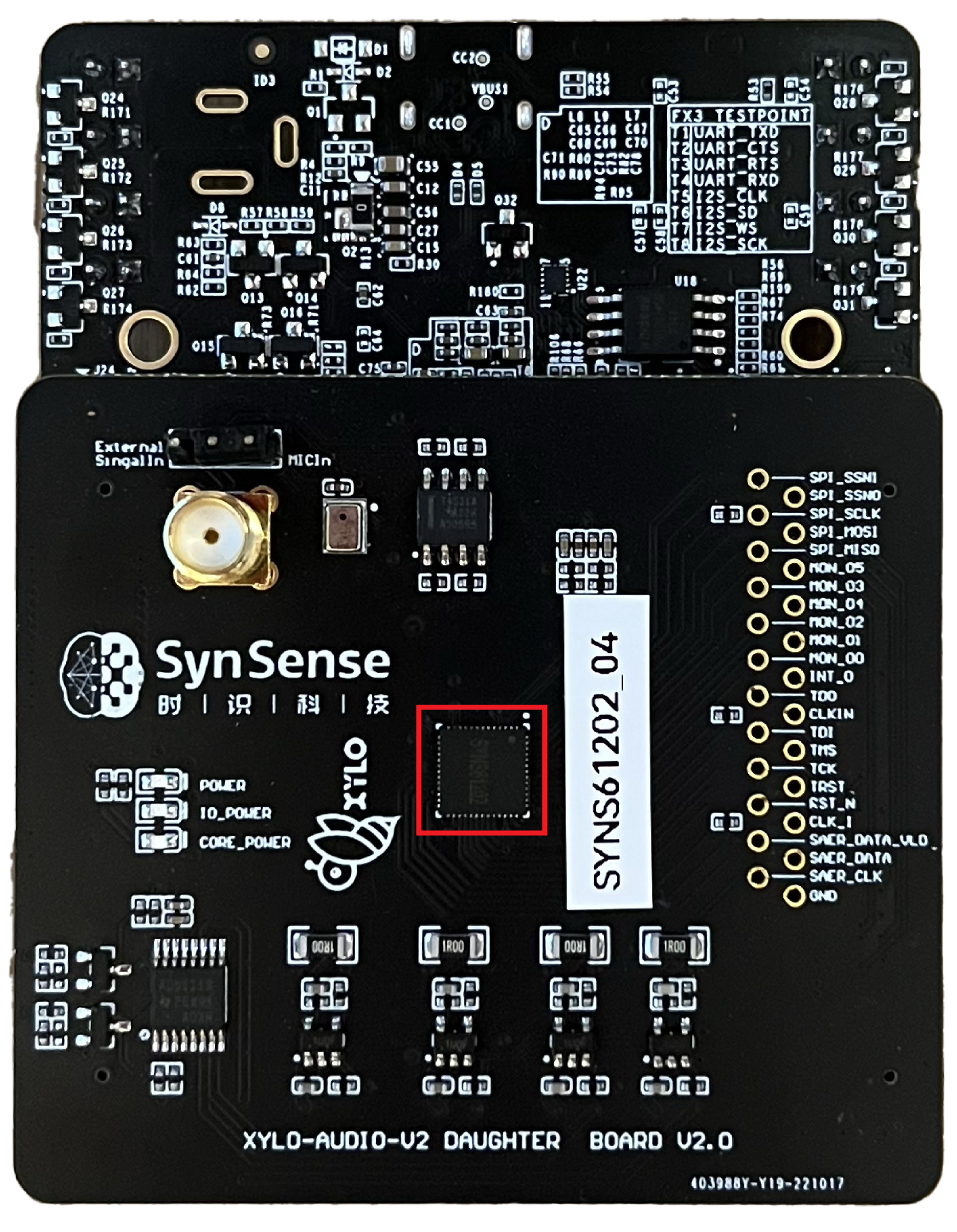
The image displays a high-resolution, top-down view of a black printed circuit board (PCB) assembly, identified as the "XYLO-AUDIO-V2 DAUGHTER BOARD V2.0". The assembly consists of a main board and a secondary board (likely an interface or bridge board) attached at the top. The board is designed for neuromorphic audio processing, featuring a central processing chip, various power management components, and an extensive array of test points for debugging and signal monitoring.
### Components/Axes
The board is organized into functional regions:
**1. Top Section (Interface/Bridge Board):**
* **FX3 TESTPOINT Block (Top Right):** A cluster of test points labeled:
* T1 UART TXD
* T2 UART CTS
* T3 UART RTS
* T4 UART RXD
* T5 I2S CLK
* T6 I2S SD
* T7 I2S WS
* T8 I2S SCK
* **Miscellaneous:** Various surface-mount capacitors, resistors, and an integrated circuit (U18) are visible.
**2. Main Board (Center/Left):**
* **Branding:** "SynSense" logo accompanied by Chinese characters: **时 | 识 | 科 | 技** (Translation: Time | Knowledge | Science | Technology).
* **Product Logo:** "XYLO" logo (stylized bee/insect icon).
* **Input/Power:**
* "External Signal In" and "MICIn" (Microphone Input) near a gold SMA connector.
* Power rail indicators: "POWER", "IO_POWER", "CORE_POWER".
* **Central Processor:** A square integrated circuit located in the center of the board, highlighted by a red square border.
* **Identification Label:** A white sticker reading "SYN61202_04".
**3. Main Board (Right - Pinout/Test Points):**
A vertical column of 24 test points/pins, labeled from top to bottom:
* SPI_SSN1
* SPI_SSN0
* SPI_SCLK
* SPI_MOSI
* SPI_MISO
* MON_05
* MON_03
* MON_04
* MON_02
* MON_01
* MON_00
* INT_0
* TDO
* CLKIN
* TDI
* TMS
* TCK
* TRST
* RST_N
* CLK_I
* SAER_DATA_VLD
* SAER_DATA
* SAER_CLK
* GND
**4. Footer:**
* "XYLO-AUDIO-V2 DAUGHTER BOARD V2.0"
* "403988Y-Y19-221017" (Serial/Part number)
### Detailed Analysis
* **Language:** The Chinese characters "时 | 识 | 科 | 技" are present. These translate to "Time | Knowledge | Science | Technology," which aligns with the "SynSense" brand identity (a neuromorphic computing company).
* **Connectivity:** The board is heavily focused on connectivity. The presence of "FX3" test points suggests the board is designed to interface with a Cypress/Infineon FX3 USB 3.0 peripheral controller, which is common for high-speed data streaming from sensors.
* **Neuromorphic Indicators:** The labels "SAER_DATA" (SynSense Asynchronous Event Representation) and "MON_XX" (Monitor pins) are characteristic of neuromorphic hardware, which processes data as asynchronous spikes rather than traditional clocked frames.
* **Power Management:** The board includes dedicated power rails (POWER, IO_POWER, CORE_POWER), suggesting the need for distinct voltage domains for the analog/sensor front-end and the digital processing core.
### Key Observations
* **Red Box:** The red box highlights the primary processing chip (likely the XYLO chip itself).
* **Modularity:** The board is explicitly labeled as a "Daughter Board," indicating it is intended to be plugged into a larger "Motherboard" or evaluation system.
* **Debugging:** The high density of test points (UART, I2S, SPI, JTAG/SWD, and Monitor pins) indicates this is an engineering/development version of the hardware, not a final consumer product.
### Interpretation
This image depicts a development platform for SynSense's neuromorphic audio processing technology.
* **Functionality:** The board is designed to ingest audio signals (via MICIn or External Signal In), process them using the central chip (SYN61202), and output the processed data—likely in an event-based format (SAER)—to an external host via the SPI or I2S interfaces.
* **Peircean Investigative View:** The presence of "FX3" test points and "SAER" pins suggests a high-bandwidth data pipeline. The board is designed to bridge the gap between raw analog audio input and digital event-based processing. The "Daughter Board" designation implies that the user is expected to provide the power and host-interface logic (likely via the FX3 controller) on a separate carrier board, allowing the user to swap out different sensor or processing modules easily. The board is a tool for rapid prototyping and algorithm validation in the field of neuromorphic engineering.