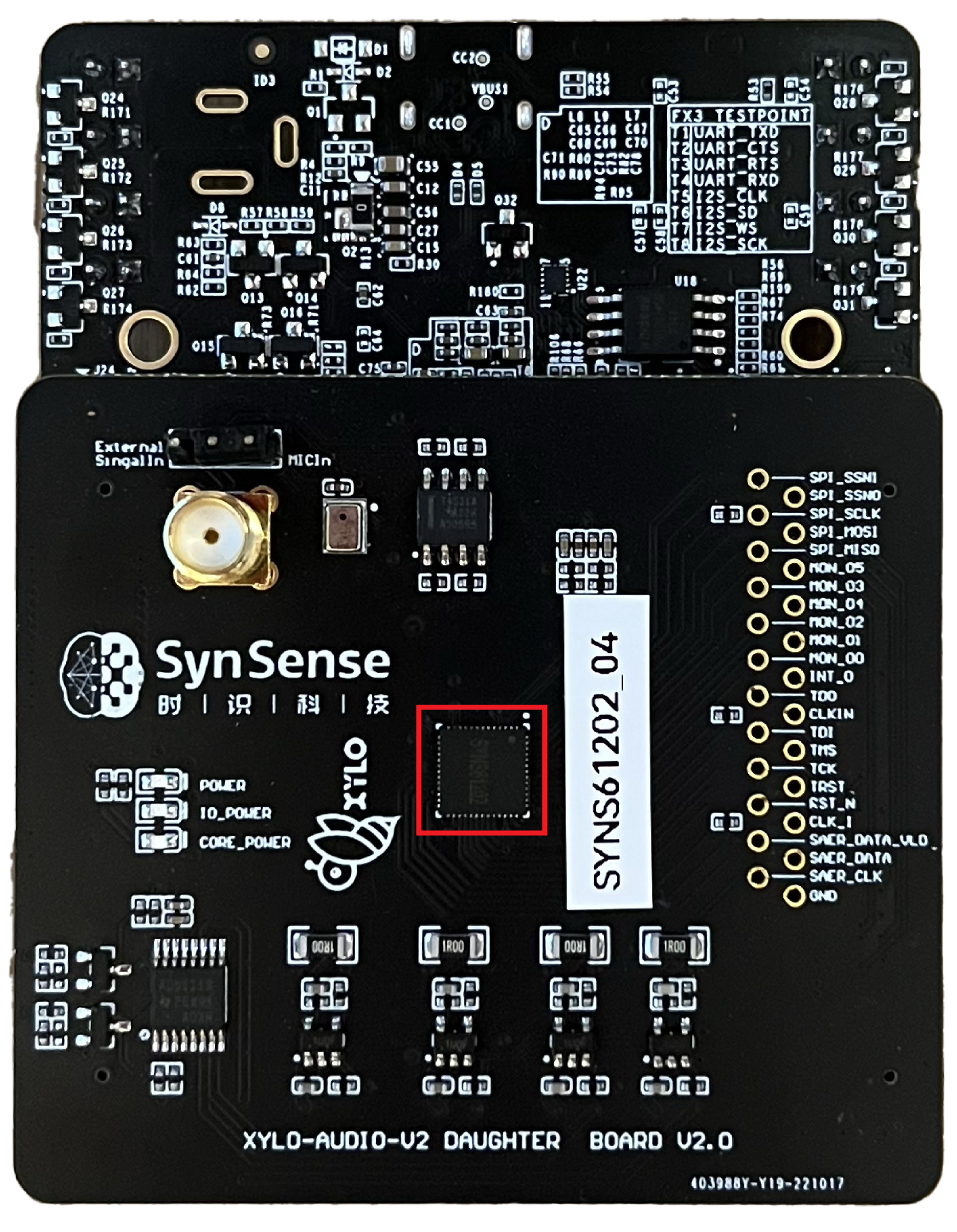
## Circuit Board: SynSense XYLO-AUDIO-V2 Daughter Board V2.0
### Overview
The image displays a two-part printed circuit board (PCB) assembly, consisting of a smaller top board mounted onto a larger main daughter board. The board is black with white silkscreen labeling and gold-plated pads and connectors. It appears to be an audio processing or development board, as indicated by its name and components. The primary language of the text is English, with some Chinese characters present.
### Components and Labels
#### Main Board (Bottom Section)
* **Board Name & Version:** Located at the bottom edge: `XYLO-AUDIO-V2 DAUGHTER BOARD V2.0`.
* **Manufacturer/Brand:** Prominent logo and text on the left side: `SynSense` with Chinese characters `时 | 识 | 科 | 技` below it (Translation: Time | Perception | Science | Technology).
* **Product Line Logo:** A bee logo with the text `XYLO` next to it.
* **Serial/Part Number Sticker:** A white vertical sticker on the right side reads `SYNS61202_04`.
* **Main Processor (Highlighted):** A large square integrated circuit (IC) in the center, outlined by a red box. The marking on the chip is partially legible as `SYNS1202`.
* **Input/Output Connectors & Labels:**
* Top-left: A 3.5mm audio jack labeled `External Signal In`.
* Next to it: A small surface-mount microphone labeled `MIC In`.
* Right edge: A 2x10 pin (20-pin) header with gold-plated through-holes. Each pin is labeled with its signal name (see detailed list below).
* **Power Section:** On the left, below the logo, three sets of pads are labeled: `POWER`, `IO_POWER`, and `CORE_POWER`.
* **Other Components:** Several smaller ICs, resistors, capacitors, and inductors are scattered across the board. Four identical sections near the bottom are labeled `1R00`, likely indicating 1-ohm resistors or current sense points.
* **Manufacturing Code:** At the very bottom right corner: `403988Y-Y19-221017`.
#### Top Board (Mounted Module)
This is a densely populated board connected to the main board. Key labels include:
* **Test Point Table:** A clearly printed table in the upper right quadrant titled `FX3 TESTPOINT`. It lists test points T1 through T8 with their corresponding signals:
| Test Point | Signal |
|------------|-------------|
| T1 | UART_TXD |
| T2 | UART_CTS |
| T3 | UART_RTS |
| T4 | UART_RXD |
| T5 | I2S_CLK |
| T6 | I2S_SD |
| T7 | I2S_WS |
| T8 | I2S_SCK |
* **Component Designators:** Hundreds of small white labels identify individual components (e.g., `R171`, `C024`, `U18`, `L6`, `Q013`). These follow standard reference designator formats (R=resistor, C=capacitor, U=integrated circuit, L=inductor, Q=transistor).
* **Other Labels:** `VBUS1`, `CC1`, `CC2`, `ID3`, `J24`.
### Detailed Analysis: Pin Header Labels (Right Edge of Main Board)
The 20-pin header on the right side of the main board has the following signal labels, listed from top to bottom:
1. `SPI_SSNI`
2. `SPI_SSNO`
3. `SPI_SCLK`
4. `SPI_MOSI`
5. `SPI_MISO`
6. `MON_05`
7. `MON_03`
8. `MON_04`
9. `MON_02`
10. `MON_01`
11. `MON_00`
12. `INT_0`
13. `TDO`
14. `CLKIN`
15. `TDI`
16. `TMS`
17. `TCK`
18. `TRST`
19. `RST_N`
20. `CLK_I`
21. `SAER_DATA_VLD`
22. `SAER_DATA`
23. `SAER_CLK`
24. `GND`
*(Note: The header appears to have 20 physical pins, but 24 labels are printed. The labels `SAER_DATA_VLD`, `SAER_DATA`, `SAER_CLK`, and `GND` are grouped at the bottom, suggesting they may correspond to the last few pins or a separate connector pad.)*
### Key Observations
1. **Dual-Board Architecture:** The design separates a dense, likely digital or power management section (top board) from the main audio I/O and processing section (bottom board).
2. **Comprehensive Debug Interface:** The `FX3 TESTPOINT` table and the extensive pin header provide direct access to UART, I2S (audio), SPI, JTAG (`TDO`, `TDI`, `TMS`, `TCK`, `TRST`), and monitoring signals, indicating this is a development or evaluation board.
3. **Audio Focus:** The presence of an `External Signal In` jack, `MIC In`, and I2S test points strongly suggests the board's primary function is audio signal acquisition and processing.
4. **Main IC:** The centrally placed `SYNS1202` chip (highlighted) is almost certainly the main audio processor or system-on-chip (SoC) for this board.
5. **Power Domains:** The separate `POWER`, `IO_POWER`, and `CORE_POWER` labels indicate multiple regulated voltage domains, typical for complex digital systems.
### Interpretation
This is a **development or daughter board for audio processing**, likely based on a SynSense (formerly known as a Chinese AI chip company) `SYNS1202` processor. The "XYLO" branding may refer to a specific product line or technology.
The board is designed for integration and testing. The top "FX3" board likely handles USB connectivity (suggested by `VBUS`, `CC` labels common in USB-C) or acts as a bridge/FPGA for the main processor, given its dense layout and dedicated test points for communication protocols.
The extensive pin header exposes all critical interfaces: SPI for peripheral communication, multiple monitor (`MON`) and interrupt (`INT`) lines, JTAG for debugging the main processor, and audio-specific I2S and "SAER" (possibly a proprietary audio interface) signals. This allows engineers to connect the board to an oscilloscope, logic analyzer, or a host system for software development, signal integrity testing, and system integration.
The manufacturing code `403988Y-Y19-221017` suggests a production date around late 2021 (week 22 of 2021 or October 2022, depending on the date format). The sticker `SYNS61202_04` is likely a unique serial number or batch identifier for the specific unit or main IC.