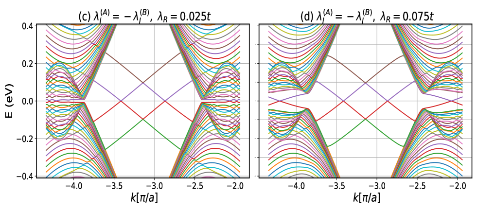
# Technical Data Extraction: Electronic Band Structure Plots
This document provides a detailed technical extraction of the information contained in the provided image, which consists of two side-by-side electronic band structure plots (labeled 'c' and 'd').
## 1. General Metadata and Axis Information
The image displays two subplots representing energy ($E$) versus wavevector ($k$).
* **Vertical Axis (Y-axis):**
* **Label:** $E \text{ (eV)}$
* **Range:** $-0.4$ to $0.4$
* **Major Tick Marks:** $-0.4, -0.2, 0.0, 0.2, 0.4$
* **Horizontal Axis (X-axis):**
* **Label:** $k [\pi/a]$
* **Range:** Approximately $-4.4$ to $-1.8$
* **Major Tick Marks:** $-4.0, -3.5, -3.0, -2.5, -2.0$
* **Grid:** Both plots feature a light gray rectangular grid aligned with the major tick marks.
---
## 2. Subplot (c) Analysis
### Header Information
* **Label:** (c)
* **Parameters:** $\lambda_I^{(A)} = -\lambda_I^{(B)}, \lambda_R = 0.025t$
### Component Isolation and Trends
Subplot (c) shows a band structure with a distinct bulk gap and topological edge states.
* **Bulk Bands (Dense regions):**
* Located primarily around $k \approx -3.9$ and $k \approx -2.4$.
* **Trend:** These bands form "V" shapes (conduction bands) and inverted "V" shapes (valence bands) that converge toward $E = 0$ but remain separated by a small energy gap.
* The bands are multi-colored, indicating a manifold of states.
* **Edge States (Crossing lines):**
* Four distinct linear bands cross the gap between the bulk manifolds.
* **Purple Line:** Slopes upward from left to right, crossing $E=0$ at $k \approx -3.2$.
* **Brown Line:** Slopes downward from left to right, crossing $E=0$ at $k \approx -3.2$.
* **Red Line:** Slopes downward from left to right, crossing $E=0$ at $k \approx -2.8$.
* **Green Line:** Slopes upward from left to right, crossing $E=0$ at $k \approx -2.8$.
* **Gap Characteristics:**
* The bulk gap is centered at $E = 0$.
* The crossing points of the edge states (Dirac points) are located exactly at $E = 0$ for $k \approx -3.2$ and $k \approx -2.8$.
---
## 3. Subplot (d) Analysis
### Header Information
* **Label:** (d)
* **Parameters:** $\lambda_I^{(A)} = -\lambda_I^{(B)}, \lambda_R = 0.075t$
### Component Isolation and Trends
Subplot (d) shows the effect of increasing the $\lambda_R$ parameter compared to plot (c).
* **Bulk Bands:**
* The bulk bands around $k \approx -3.9$ and $k \approx -2.4$ appear more "squashed" or flattened compared to plot (c).
* **Trend:** There is a noticeable oscillation or "wavy" pattern introduced in the bands near the gap edges, particularly visible between $k = -4.4$ and $-4.0$.
* **Edge States (Crossing lines):**
* The same four colored lines (Purple, Brown, Red, Green) are present.
* **Trend:** While they still cross the gap, their slopes are modified.
* **Purple/Brown crossing:** Shifted slightly. The crossing point remains near $E=0$ but the lines show slight curvature as they approach the bulk bands.
* **Red/Green crossing:** Similar to the other pair, they maintain a crossing near $E=0$ at $k \approx -2.8$.
* **Gap Characteristics:**
* The global energy gap between the bulk valence and conduction bands appears smaller than in plot (c) due to the increased $\lambda_R$ value causing the bands to push closer to the Fermi level ($E=0$).
---
## 4. Comparative Summary
| Feature | Subplot (c) [$\lambda_R = 0.025t$] | Subplot (d) [$\lambda_R = 0.075t$] |
| :--- | :--- | :--- |
| **Bulk Band Shape** | Sharp "V" and inverted "V" | Flattened and oscillatory/wavy |
| **Bulk Gap Size** | Larger | Smaller |
| **Edge States** | Linear crossings at $E=0$ | Crossings at $E=0$ with increased curvature |
| **Symmetry** | Highly symmetric around $E=0$ | Maintains particle-hole symmetry |
**Conclusion:** The increase in the $\lambda_R$ parameter from $0.025t$ to $0.075t$ results in a narrowing of the bulk bandgap and the introduction of more complex dispersion (oscillations) in the bulk energy bands, while preserving the topological edge state crossings at the Fermi level.