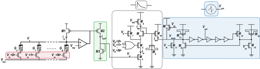
## Circuit Diagram: Memristor Crossbar Readout Circuit
### Overview
The image presents a detailed circuit diagram of a memristor crossbar readout circuit. It includes several key components: a memristor crossbar array, a buffer stage, a write pulse generator, a sense amplifier, and an output stage. The diagram illustrates the flow of signals and the interconnections between these components.
### Components/Axes
* **Memristor Crossbar Array (Left):**
* Memristors labeled as G0, G1, ..., GN.
* Input voltages: Vin<0>, Vin<1>, ..., Vin<N> at the bottom.
* Voltage Vx at the top of the memristors.
* Voltage Vbot at the bottom of the memristors.
* Current iin flowing through transistor M1.
* Voltage Vtop at the output of the op-amp.
* **Buffer Stage (Green Box):**
* Transistors M2 and M3.
* Output current ibuff.
* **Write Pulse Generator (Gray Box):**
* Transistors M4, M5, M6, M7, M8, M9, and M10.
* Input voltages: Vin<0>, Vin<1>, ..., Vin<N>.
* Voltage Vtau.
* Voltage Vg.
* Write voltage Vw.
* Output current Isyn.
* A pulse waveform is shown above the gray box.
* **Sense Amplifier and Output Stage (Blue Box):**
* Transistors M11, M12, M13, M14, M15, M16, and M17.
* Voltage Vdc.
* Voltage Vmem.
* Voltage Vik.
* Voltage Vrp.
* Output voltage Vout.
* A series of inverters are present in the middle of the blue box.
* A waveform is shown above the blue box, representing Vout.
### Detailed Analysis
* **Memristor Crossbar Array:** The array consists of N+1 memristors, each connected to a transistor. The input voltages Vin<0> to Vin<N> control the transistors, allowing current to flow through selected memristors.
* **Buffer Stage:** The buffer stage, comprising transistors M2 and M3, provides isolation and amplification for the signal coming from the memristor array. The output current ibuff is fed into the write pulse generator.
* **Write Pulse Generator:** This circuit generates a write pulse based on the input voltages and the state of the memristors. The NOR gate combines the input voltages. The transistors M4 through M10 control the timing and amplitude of the write pulse.
* **Sense Amplifier and Output Stage:** The sense amplifier detects the current flowing through the memristor array and converts it into a voltage signal. The inverters amplify and shape the signal. The transistors M14 through M16 form an output buffer to drive the output voltage Vout.
### Key Observations
* The circuit is designed to read out the state of a memristor crossbar array.
* The write pulse generator is used to program the memristors.
* The sense amplifier and output stage provide a clean and amplified output signal.
### Interpretation
The circuit diagram illustrates a complete system for reading and writing data to a memristor crossbar array. The memristor array stores data as resistance values. The buffer stage isolates the array from the write pulse generator. The write pulse generator applies appropriate voltages to program the memristors. The sense amplifier and output stage convert the resistance values into a readable voltage signal. The circuit is designed for non-volatile memory applications, where data is stored even when power is off.