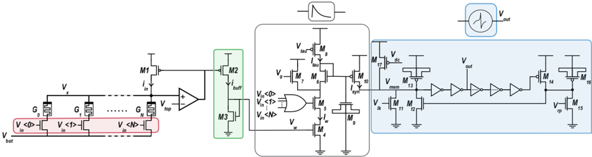
## Circuit Diagram: Voltage Buffer and Amplification Stage
### Overview
The diagram depicts a three-stage electronic circuit:
1. **Left Section (Red Box)**: Voltage divider with operational amplifier (op-amp)
2. **Middle Section (Green Box)**: Buffer stage using MOSFETs (M2, M3)
3. **Right Section (Blue Box)**: Amplification chain with multiple MOSFETs and inverters
### Components/Axes
**Left Section (Red Box):**
- **Voltage Divider**: Resistors labeled G₀, G₁, ..., Gₙ with voltage taps V₀, V₁, ..., Vₙ
- **Op-Amp**: Non-inverting configuration with input Vₓ and output V_top
- **MOSFET M1**: Connected between V_top and ground
**Middle Section (Green Box):**
- **Buffer Stage**:
- MOSFET M2: Source connected to V_in, gate to V_top, drain to V_buff
- MOSFET M3: Source grounded, gate to V_buff, drain to V_in
**Right Section (Blue Box):**
- **Amplification Chain**:
- MOSFETs M4-M16 arranged in a cascaded configuration
- Inverter stages (triangle symbols) between M5-M9 and M13-M15
- Output labeled V_out with load resistor Rₚ
### Detailed Analysis
**Left Section:**
- Voltage divider creates reference voltages V₀ to Vₙ
- Op-amp maintains V_top ≈ V_in (non-inverting gain ≈1)
- M1 acts as a current sink/sink for V_top
**Middle Section:**
- M2/M3 form a voltage follower with high input impedance
- V_buff = V_in (ideal buffer behavior)
**Right Section:**
- Cascaded MOSFETs (M4-M16) create multi-stage amplification
- Inverter stages (M5-M9, M13-M15) introduce phase shifts
- Final output V_out drives load Rₚ
### Key Observations
1. **Signal Flow**: V_in → Voltage divider → Op-amp → Buffer → Amplification chain → V_out
2. **Isolation**: Green box buffer isolates input from amplification stages
3. **Phase Shifts**: Inverter stages introduce 180° phase shifts at each stage
4. **Load Matching**: Rₚ terminates the output to prevent reflections
### Interpretation
This circuit implements a buffered, multi-stage amplifier with:
- **Input Conditioning**: Voltage divider and op-amp stabilize reference voltages
- **Isolation**: Buffer stage prevents loading effects on preceding stages
- **Gain Control**: Cascaded MOSFETs provide adjustable gain through gate-source voltages (V_gs)
- **Phase Adjustment**: Inverter stages enable precise timing control in signal processing
The design suggests applications in precision instrumentation or RF signal conditioning, where high input impedance and controlled gain are critical. The use of MOSFETs instead of BJTs indicates a preference for low noise and high input impedance characteristics.