## Memristor Crossbar Array Diagram
### Overview
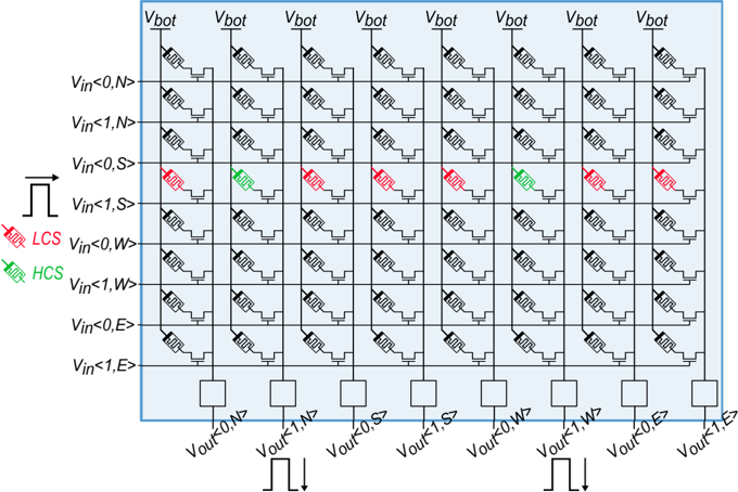
The image depicts a memristor crossbar array, a type of non-volatile memory. It shows an 8x6 grid of memristors, with input and output lines labeled. Some memristors are highlighted in red (LCS - Low Conductance State) and green (HCS - High Conductance State), indicating their state. The diagram also includes voltage source labels and pulse signal representations.
### Components/Axes
* **Grid:** An 8x6 grid representing the memristor array.
* **Memristors:** Each cell in the grid contains a memristor symbol.
* **Input Lines:** Labeled `Vin<0,N>`, `Vin<1,N>`, `Vin<0,S>`, `Vin<1,S>`, `Vin<0,W>`, `Vin<1,W>`, `Vin<0,E>`, `Vin<1,E>` on the left side of the grid.
* **Output Lines:** Labeled `Vout<0,N>`, `Vout<1,N>`, `Vout<0,S>`, `Vout<1,S>`, `Vout<0,W>`, `Vout<1,W>`, `Vout<0,E>`, `Vout<1,E>` at the bottom of the grid.
* **Voltage Source:** Labeled `Vbot` above each column of the grid.
* **Legend:** Located on the left side, indicating:
* Red: LCS (Low Conductance State)
* Green: HCS (High Conductance State)
* **Pulse Signal:** A square wave pulse signal is shown on the left side, pointing to the right, and another at the bottom, pointing downwards.
### Detailed Analysis or Content Details
* **Memristor States:**
* Row 3 (corresponding to `Vin<0,S>`): Contains one red (LCS) memristor in column 2, one green (HCS) memristor in column 3, and one red (LCS) memristor in column 5.
* Row 4 (corresponding to `Vin<1,S>`): Contains one red (LCS) memristor in column 1, one red (LCS) memristor in column 4, and one green (HCS) memristor in column 6.
* **Grid Structure:** The memristors are connected in a crossbar fashion, with horizontal lines representing input lines and vertical lines representing output lines.
* **Voltage Source Placement:** The `Vbot` voltage source is connected to the top of each column.
* **Input/Output Line Labels:** The input and output lines are labeled with a combination of 0/1 and N/S/W/E, likely representing different input/output configurations or addresses.
* **Pulse Signal Direction:** The input pulse signal points to the right, while the output pulse signal points downwards.
### Key Observations
* The memristor array is designed to store data based on the conductance state of individual memristors.
* The red and green memristors indicate the stored data pattern.
* The input and output lines are labeled in a structured manner, suggesting a specific addressing scheme.
* The pulse signals likely represent the read/write operations performed on the array.
### Interpretation
The diagram illustrates the architecture and operation of a memristor crossbar array. The array stores data by changing the conductance state of individual memristors. The input and output lines allow for addressing and accessing specific memristors within the array. The `Vbot` voltage source provides the necessary voltage for reading and writing data. The pulse signals represent the timing and direction of the read/write operations. The specific pattern of LCS and HCS memristors represents a particular data pattern stored in the array. The N/S/W/E notation in the input/output labels might refer to different directions or polarities of the applied voltage or current. The 0/1 notation might refer to different voltage levels or binary states.