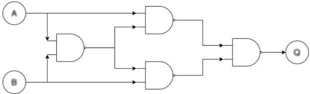
## Digital Logic Circuit Diagram: Combinational Logic Structure
### Overview
The image depicts a digital logic circuit composed of multiple AND gates, input nodes (A and B), and an output node (Q). The diagram illustrates the flow of logical signals through interconnected gates, with no explicit numerical data or trends.
### Components/Axes
- **Inputs**:
- Node **A** (top-left)
- Node **B** (bottom-left)
- **Output**:
- Node **Q** (rightmost)
- **Logic Gates**:
- All gates are **AND gates** (standard symbol: triangle with flat edge).
- No explicit labels for individual gates (e.g., G1, G2), but their connections are visually distinct.
### Detailed Analysis
1. **Input Connections**:
- **A** is connected to two AND gates:
- One directly to the first gate (G1).
- Another to a gate further downstream (G3).
- **B** is connected to two AND gates:
- One directly to G1.
- Another to a gate further downstream (G2).
2. **Gate Connections**:
- **G1**: Combines **A** and **B** (output feeds into G2 and G3).
- **G2**: Combines output of G1 and **B** (output feeds into G4).
- **G3**: Combines output of G1 and **A** (output feeds into G4).
- **G4**: Combines outputs of G2 and G3 (output feeds into G5).
- **G5**: Combines output of G4 and **A** (final output **Q**).
3. **Flow Direction**:
- Signals flow from **A** and **B** through sequential AND gates, with intermediate outputs feeding into subsequent gates.
- Final output **Q** is derived from the combination of all intermediate gate outputs and **A**.
### Key Observations
- The circuit uses **only AND gates**, with no OR, NOT, or other gate types visible.
- The structure suggests a **combinational logic** design, where the output **Q** depends solely on the current inputs **A** and **B**.
- No feedback loops or sequential elements (e.g., flip-flops) are present.
### Interpretation
This diagram represents a **combinational logic circuit** that processes inputs **A** and **B** through a series of AND gates to produce output **Q**. The specific Boolean function implemented depends on the arrangement of gates:
- **G1** computes **A ∧ B**.
- **G2** computes **(A ∧ B) ∧ B** (equivalent to **A ∧ B**).
- **G3** computes **(A ∧ B) ∧ A** (equivalent to **A ∧ B**).
- **G4** combines G2 and G3 outputs: **(A ∧ B) ∧ (A ∧ B)** (still **A ∧ B**).
- **G5** combines G4 output with **A**: **(A ∧ B) ∧ A** (equivalent to **A ∧ B**).
Thus, the final output **Q** simplifies to **A ∧ B**, indicating the circuit acts as a basic AND gate. However, the redundant gates suggest potential optimization opportunities or a placeholder for more complex logic.
No numerical data, trends, or anomalies are present in the diagram. The focus is purely on the structural relationships between inputs, gates, and output.