## Conductance vs. Programming Current and Device State
### Overview
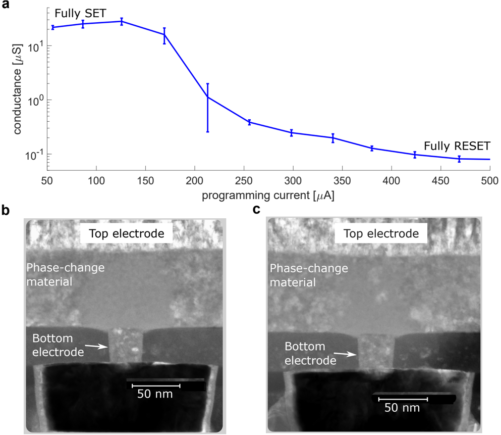
The image presents a graph showing the relationship between conductance and programming current, along with two transmission electron microscopy (TEM) images illustrating the device's state. The graph (a) plots conductance (in microSiemens) against programming current (in microAmperes). Images (b) and (c) show the device structure, including the top electrode, phase-change material, and bottom electrode, with a scale bar indicating 50 nm.
### Components/Axes
**Graph (a):**
* **X-axis:** programming current [μA]. Scale ranges from 50 to 500 in increments of 50.
* **Y-axis:** conductance [μS]. Logarithmic scale ranging from 0.1 to 10.
* **Data Series:** A single blue line with error bars representing the conductance as a function of programming current.
* **Annotations:** "Fully SET" is located at the top-left of the graph, indicating the device's state at low programming currents. "Fully RESET" is located at the top-right of the graph, indicating the device's state at high programming currents.
**TEM Images (b) and (c):**
* **Labels:** "Top electrode", "Phase-change material", "Bottom electrode".
* **Scale Bar:** 50 nm.
### Detailed Analysis
**Graph (a):**
* **Trend:** The blue line shows a decreasing trend in conductance as the programming current increases.
* **Data Points:**
* At 50 μA, conductance is approximately 15 μS.
* At 100 μA, conductance is approximately 15 μS.
* At 150 μA, conductance is approximately 14 μS.
* At 200 μA, conductance is approximately 2 μS.
* At 250 μA, conductance is approximately 0.3 μS.
* At 300 μA, conductance is approximately 0.2 μS.
* At 350 μA, conductance is approximately 0.15 μS.
* At 400 μA, conductance is approximately 0.12 μS.
* At 450 μA, conductance is approximately 0.11 μS.
* At 500 μA, conductance is approximately 0.1 μS.
* **Error Bars:** Error bars are present at each data point, indicating the uncertainty in the conductance measurements. The error bars are larger around 200 μA.
**TEM Images (b) and (c):**
* The images show the cross-sectional view of the device.
* The top electrode, phase-change material, and bottom electrode are clearly labeled.
* The scale bar indicates that the width of the bottom electrode is approximately 50 nm.
* The images appear to show different states of the phase-change material, potentially corresponding to the SET and RESET states.
### Key Observations
* The conductance decreases significantly as the programming current increases from 150 μA to 250 μA.
* The device transitions from a "Fully SET" state (high conductance) to a "Fully RESET" state (low conductance) as the programming current increases.
* The TEM images provide a visual representation of the device structure and potentially the phase-change material's state.
### Interpretation
The data suggests that the programming current controls the conductance of the device, likely by inducing a phase change in the phase-change material. At low programming currents, the device is in the SET state, characterized by high conductance. As the programming current increases, the phase-change material transitions to a RESET state, resulting in a significant decrease in conductance. The TEM images likely show the structural differences between the SET and RESET states of the phase-change material. The error bars indicate the variability in the conductance measurements, which is more pronounced during the transition between the SET and RESET states.