\n
## Chart/Diagram Type: Conductance vs. Programming Current & TEM Images of Phase-Change Material
### Overview
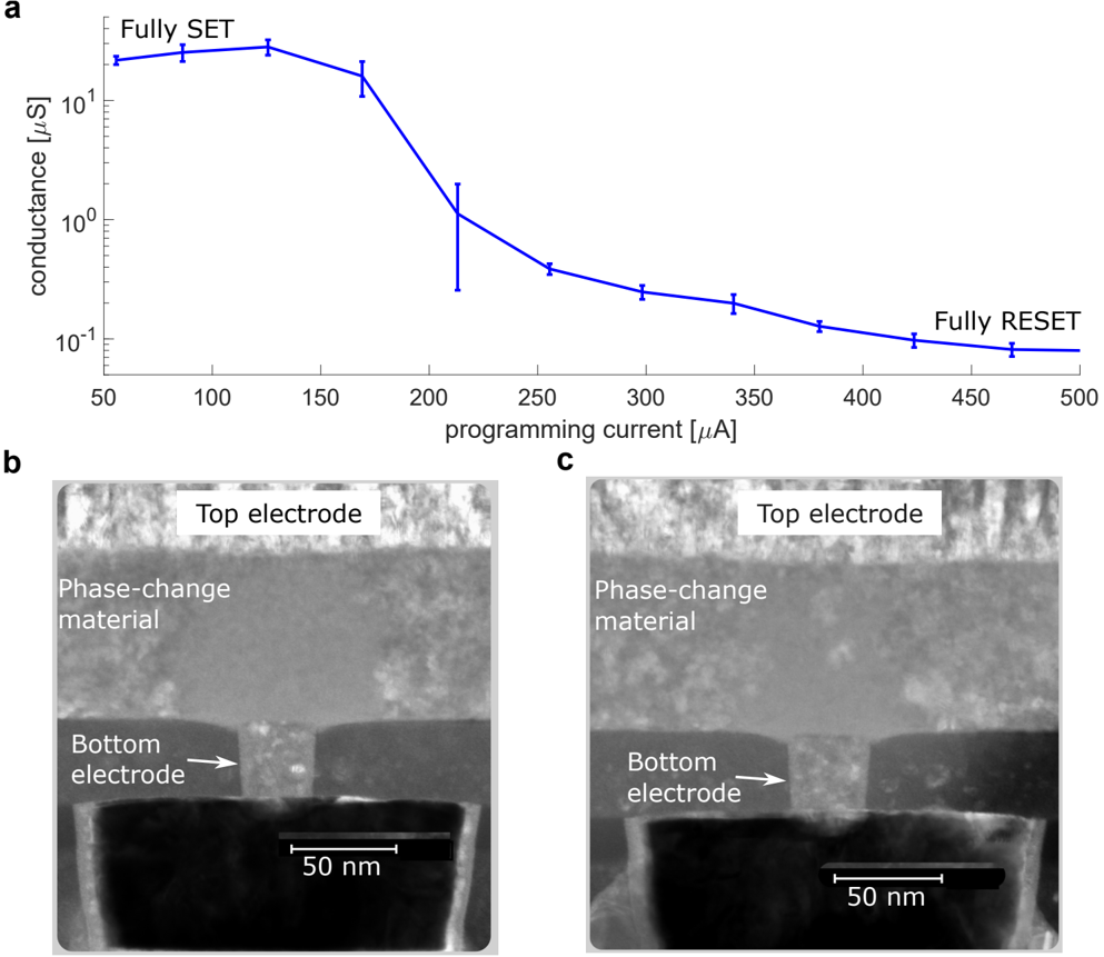
The image presents a graph illustrating the relationship between conductance and programming current for a phase-change material. Below the graph are two Transmission Electron Microscopy (TEM) images showing the device structure in different states. The graph demonstrates a switching behavior, where conductance decreases with increasing programming current. The TEM images provide a visual representation of the device's physical structure.
### Components/Axes
* **Graph (a):**
* **X-axis:** Programming Current [µA], ranging from approximately 50 to 500.
* **Y-axis:** Conductance [µS], on a logarithmic scale, ranging from approximately 10 to 1000.
* **Data Series:** A single blue line with error bars representing conductance as a function of programming current.
* **Labels:** "Fully SET" at the left end of the curve (approximately 100 µA, 1000 µS), "Fully RESET" at the right end of the curve (approximately 450 µA, 10 µS).
* **TEM Image (b):**
* **Labels:** "Top electrode", "Phase-change material", "Bottom electrode".
* **Scale Bar:** 50 nm.
* **TEM Image (c):**
* **Labels:** "Top electrode", "Phase-change material", "Bottom electrode".
* **Scale Bar:** 50 nm.
### Detailed Analysis or Content Details
* **Graph (a):**
* The line starts at approximately (100 µA, 1000 µS) labeled "Fully SET".
* The line exhibits a steep decrease in conductance between approximately 150 µA and 250 µA.
* The conductance plateaus around approximately 250 µA to 350 µA, with a conductance value of around 20 µS.
* The line continues to decrease, reaching approximately (450 µA, 10 µS) labeled "Fully RESET".
* Error bars are present throughout the graph, indicating uncertainty in the conductance measurements. The error bars are approximately ± 2 µS around 250 µA.
* **TEM Image (b):**
* Shows a cross-sectional view of the device.
* The top electrode is visible at the top of the image.
* The phase-change material is located between the top and bottom electrodes.
* The bottom electrode is visible at the bottom of the image.
* The dimensions of the phase-change material are approximately 50 nm x 50 nm.
* **TEM Image (c):**
* Similar to (b), showing a cross-sectional view of the device.
* The structure appears slightly different, potentially representing a different state of the phase-change material.
* The dimensions of the phase-change material are approximately 50 nm x 50 nm.
### Key Observations
* The graph demonstrates a clear switching behavior, with a significant drop in conductance as the programming current increases.
* The TEM images reveal the layered structure of the device, consisting of a top electrode, phase-change material, and bottom electrode.
* The TEM images suggest a change in the phase-change material's structure between images (b) and (c).
### Interpretation
The data suggests that the phase-change material exhibits resistive switching behavior. Applying a programming current causes a change in the material's state, leading to a decrease in conductance. The "Fully SET" state represents a high-conductance state, while the "Fully RESET" state represents a low-conductance state. The TEM images provide visual confirmation of the device structure and potentially illustrate the structural changes occurring during the switching process. The difference between TEM images (b) and (c) could represent the amorphous and crystalline states of the phase-change material, respectively. The error bars on the graph indicate that the switching behavior is not perfectly deterministic and there is some variability in the conductance values. This is typical for phase-change memory devices. The scale bars on the TEM images indicate the nanoscale dimensions of the device, highlighting its potential for high-density memory applications.