## Phase-Change Memory Device Characterization: Conductance vs. Programming Current and Cross-Sectional Microscopy
### Overview
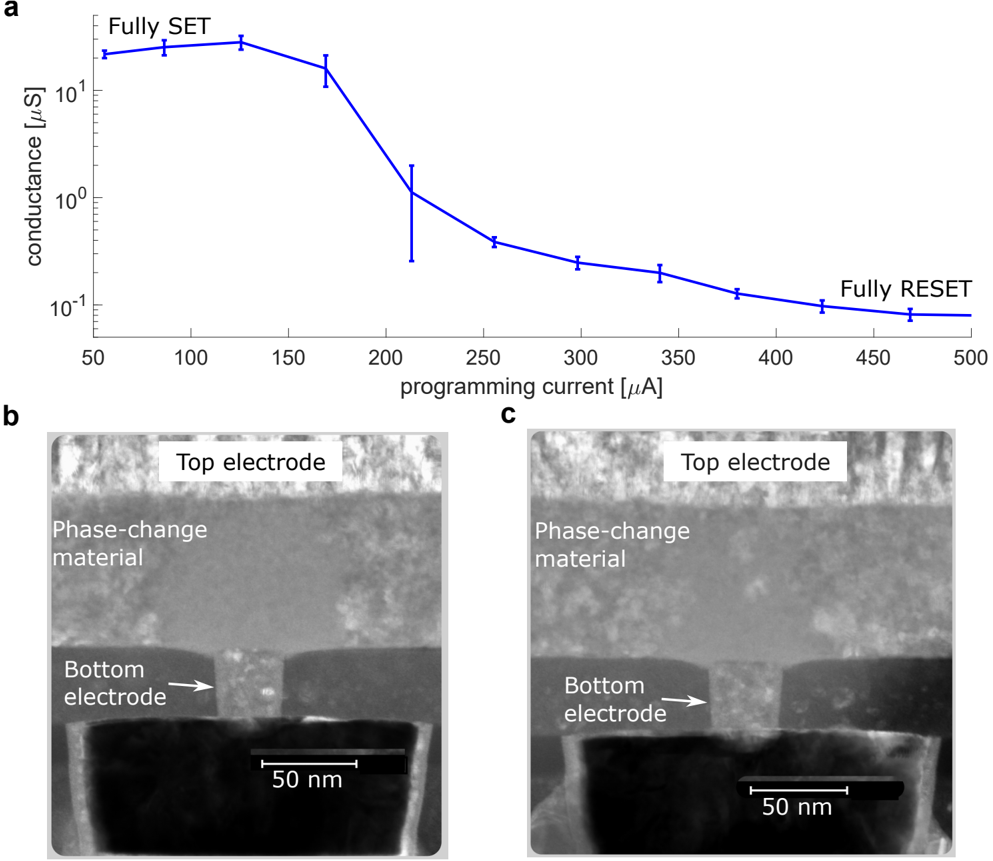
The image is a composite figure, likely from a scientific publication, containing three panels labeled **a**, **b**, and **c**. Panel **a** is a line graph plotting electrical conductance against programming current for a phase-change memory (PCM) device. Panels **b** and **c** are cross-sectional microscopy images (likely Transmission Electron Microscopy - TEM) showing the physical structure of the device in two different states.
### Components/Axes
**Panel a: Line Graph**
* **Title/Annotation (Top Left):** "Fully SET"
* **Title/Annotation (Bottom Right):** "Fully RESET"
* **Y-axis:**
* **Label:** `conductance [µS]` (microsiemens)
* **Scale:** Logarithmic (base 10). Major ticks at 10⁻¹, 10⁰, 10¹.
* **X-axis:**
* **Label:** `programming current [µA]` (microamperes)
* **Scale:** Linear. Major ticks at 50, 100, 150, 200, 250, 300, 350, 400, 450, 500.
* **Data Series:** A single blue line with error bars (vertical lines indicating standard deviation or range).
**Panel b: Microscopy Image (Left)**
* **Labels (Top to Bottom):**
* `Top electrode` (white text on dark background, top center)
* `Phase-change material` (white text, middle left)
* `Bottom electrode` (white text, lower left, with a white arrow pointing right towards a dark, narrow feature)
* **Scale Bar:** Located in the bottom right corner. White line with text `50 nm` below it.
**Panel c: Microscopy Image (Right)**
* **Labels (Top to Bottom):**
* `Top electrode` (white text on dark background, top center)
* `Phase-change material` (white text, middle left)
* `Bottom electrode` (white text, lower left, with a white arrow pointing right towards a dark, narrow feature)
* **Scale Bar:** Located in the bottom right corner. White line with text `50 nm` below it.
### Detailed Analysis
**Panel a: Conductance vs. Programming Current**
* **Trend Verification:** The blue line shows a clear, non-linear decreasing trend. Conductance starts high at low programming currents and decreases as the current increases, with the steepest drop occurring between approximately 175 µA and 225 µA.
* **Data Points (Approximate, read from log-linear plot):**
* At ~50 µA: Conductance ≈ 20 µS (Fully SET state).
* At ~125 µA: Conductance ≈ 25 µS (peak value).
* At ~175 µA: Conductance ≈ 15 µS.
* At ~215 µA: Conductance ≈ 1 µS. This point has a very large error bar, spanning from ~0.3 µS to ~3 µS, indicating high variability in this transition region.
* At ~255 µA: Conductance ≈ 0.4 µS.
* At ~300 µA: Conductance ≈ 0.25 µS.
* At ~340 µA: Conductance ≈ 0.2 µS.
* At ~380 µA: Conductance ≈ 0.15 µS.
* At ~425 µA: Conductance ≈ 0.1 µS.
* At ~470 µA: Conductance ≈ 0.09 µS (Fully RESET state).
**Panels b & c: Device Cross-Sections**
* **Component Isolation (Common Structure):** Both images show a layered structure from top to bottom: a dark, granular "Top electrode", a lighter gray, uniform "Phase-change material" layer, and a patterned "Bottom electrode" structure. The bottom electrode appears as a dark, narrow pillar or heater contact, pointed to by the arrow.
* **Visual Comparison (b vs. c):**
* **Panel b:** The phase-change material layer appears relatively uniform in contrast. This likely corresponds to the crystalline (SET) state, which is more conductive.
* **Panel c:** The phase-change material layer directly above the bottom electrode contact shows a distinct, darker, and more amorphous-looking region. This localized change in material structure is characteristic of the RESET operation, where the material is melted and quenched into an amorphous, high-resistivity state.
* **Spatial Grounding:** The scale bar in both images is placed in the bottom-right quadrant. The "Bottom electrode" label and arrow are consistently placed in the lower-left quadrant, pointing to the central electrode feature.
### Key Observations
1. **Threshold Switching:** The graph in panel **a** demonstrates a clear threshold behavior. The device maintains high conductance (SET state) up to a programming current of about 175 µA. Beyond this point, conductance drops sharply by over an order of magnitude, indicating the transition to the RESET state.
2. **State Variability:** The large error bar at ~215 µA suggests the RESET process is stochastic or highly sensitive to exact conditions in the transition region. The final RESET state (at >400 µA) shows much smaller error bars, indicating a stable, reproducible low-conductance state.
3. **Structural Correlation:** The microscopy images provide a physical basis for the electrical data. The uniform material in **b** (SET) correlates with high conductance, while the formation of a localized amorphous dome in **c** (RESET) correlates with low conductance, as the amorphous phase has much higher electrical resistivity.
### Interpretation
This figure comprehensively characterizes the switching operation of a phase-change memory cell. The electrical data in **a** quantifies the fundamental memory window: the ratio between the high-conductance (logic '1') SET state and the low-conductance (logic '0') RESET state is approximately 200:1 (20 µS vs. 0.1 µS). This large on/off ratio is desirable for reliable data storage and readout.
The transition is not instantaneous but occurs over a range of programming currents, with a critical threshold around 200 µA. The high variability in this region is a known challenge in PCM technology, related to the dynamics of melt/quench processes.
The cross-sectional images (**b** and **c**) serve as direct physical evidence, linking the electrical behavior to a structural phase change. They confirm that the RESET operation involves the creation of a high-resistivity amorphous region precisely at the location of current injection (the bottom electrode), which is the intended mechanism for this type of memory. The scale bars confirm the active switching volume is on the nanometer scale (~50-100 nm), highlighting the high-density potential of the technology.
**Language Declaration:** All text in the image is in English.