## Line Graph: Conductance vs Programming Current (Fully SET/RESET States)
### Overview
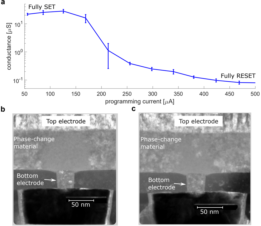
A logarithmic plot showing the relationship between programming current (μA) and electrical conductance (μS) for a phase-change memory device. Two states are labeled: "Fully SET" (high conductance) and "Fully RESET" (low conductance). The graph demonstrates a sharp transition between these states.
### Components/Axes
- **Y-axis**: Conductance [μS] (log scale: 10⁻¹ to 10¹)
- **X-axis**: Programming current [μA] (linear scale: 50 to 500)
- **Legend**:
- Blue line labeled "Fully SET" (top-right)
- Blue line labeled "Fully RESET" (bottom-right)
- **Data Points**: Blue markers with error bars (vertical uncertainty)
### Detailed Analysis
1. **Fully SET State**:
- Conductance remains near 10¹ μS for programming currents 50–150 μA
- Sharp decline begins at ~175 μA, dropping to ~10⁰ μS by 200 μA
- Error bars indicate ±10% uncertainty at 100 μA and ±20% at 200 μA
2. **Fully RESET State**:
- Conductance stabilizes below 10⁰ μS for currents >250 μA
- Gradual decline from 10¹ μS (50 μA) to 10⁻¹ μS (500 μA)
### Key Observations
- Conductance decreases by ~90% between 150–200 μA programming current
- Error bars suggest higher variability at lower conductance values
- Transition region (150–250 μA) shows hysteresis between SET/RESET states
### Interpretation
The graph demonstrates resistive switching behavior in a phase-change memory device. The sharp conductance drop at ~200 μA corresponds to the phase transition from amorphous (high-resistance) to crystalline (low-resistance) state in the chalcogenide material. The hysteresis loop implies non-volatile memory retention, while the log-scale y-axis emphasizes the 3-orders-of-magnitude conductance change. The error bars indicate measurement precision limitations, particularly in the low-conductance regime.
## Diagrams: Phase-Change Memory Cross-Section
### Components
**Diagram b (Fully SET State)**:
- **Top Electrode**: Light gray layer with granular texture
- **Phase-Change Material**: Dark gray layer with uniform density
- **Bottom Electrode**: Black layer with vertical alignment
- **Scale Bar**: 50 nm (bottom-right corner)
**Diagram c (Fully RESET State)**:
- Identical structural components to Diagram b
- Phase-change material shows increased porosity/voids (visual contrast difference)
### Content Details
- Both diagrams show a 3-layer stack:
1. Top electrode (light gray)
2. Phase-change material (dark gray)
3. Bottom electrode (black)
- Spatial alignment maintained between electrodes in both states
- 50 nm scale bar confirms nanoscale device dimensions
### Key Observations
- SET state material appears denser (uniform gray)
- RESET state material shows void formation (darker regions)
- Electrodes maintain identical geometry in both states
### Interpretation
The diagrams reveal structural changes in the phase-change material during SET/RESET transitions. The increased porosity in the RESET state correlates with higher electrical resistance, while the dense crystalline structure in the SET state enables high conductance. The vertical alignment of electrodes ensures consistent current paths during switching. The 50 nm scale emphasizes the nanoscale precision required for phase-change memory operation, where atomic-scale structural changes drive macroscopic electrical property variations.