## System Architecture Diagram: Multi-Level Memory Hierarchy
### Overview
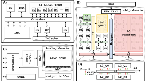
The image presents a system architecture diagram showcasing a multi-level memory hierarchy. It consists of four sub-diagrams (A, B, C, and D) illustrating different aspects of the system's memory organization and data flow. The architecture includes components such as L1 Local TCDM, Crossbar, IMA, I-Cache, HBM, L1/L2/L3 caches, AIMC CORE, and associated control and data paths.
### Components/Axes
**A) Local TCDM and Crossbar:**
* **L1 Local TCDM:** Contains blocks labeled B0, B1, B2, B3, B4, ..., BN.
* **EV:** Connected to the Crossbar.
* **DMA:** Connected to the Crossbar.
* **Crossbar:** Interconnects L1 Local TCDM, EV, DMA, IMA, and RV blocks.
* **IMA:** Connected to the Crossbar.
* **RV:** Multiple instances connected to the Crossbar and I-Cache.
* **I-Cache:** Connected to the RV blocks.
**B) HBM and Cache Hierarchy:**
* **HBM:** High Bandwidth Memory at the top.
* **HBM Ctrl:** HBM Controller, connected to HBM and the Wrapper.
* **Chip Domain:** Enclosed by a dotted line, containing the cache hierarchy.
* **L1 quad:** Four L1 cache blocks (labeled "L1") arranged in a square, each connected to a "CL" block. The L1 quad is colored green.
* **L2 quad:** A yellow block labeled "L2 quad".
* **L2:** Vertical yellow block connecting L1 quads and L3 blocks. Each L1 quad is connected to the L2 block via a "CL" block.
* **L3 quadrant:** A red block labeled "L3 quadrant".
* **L3:** Horizontal red blocks connecting the L2 block to the L3 quadrant.
* **Wrapper:** A blue vertical block connecting HBM Ctrl to the L3 blocks.
* **CL:** Small blocks connecting L1 quads to L2 and L2 to L3.
**C) Analog Domain and Streamers:**
* **Streamers:** Block on the left, connected to the input buffer.
* **Input Buffer:** Connected to the Streamers and DAC.
* **Analog Domain:** Enclosed by a dotted line.
* **AIMC CORE:** Core component within the Analog Domain.
* **DAC:** Digital-to-Analog Converter, connected to the Input Buffer and AIMC CORE.
* **ADC:** Analog-to-Digital Converter, connected to the AIMC CORE and Output Buffer.
* **Output Buffer:** Connected to the ADC and CTRL.
* **CTRL:** Control block, connected to Streamers and Output Buffer.
**D) L2/L3 Interconnection:**
* **L2_Q0, L2_Q1, L2_Q2, L2_Q3:** Four blocks representing L2 quadrants.
* **L2:** Central block connecting the L2 quadrants.
* **L3:** Block connected to the L2 block.
* **M -> S:** Direction indicator.
* **Write:** Green arrows indicating write direction.
* **Read:** Red arrows indicating read direction.
### Detailed Analysis or ### Content Details
**A) Local TCDM and Crossbar:**
* The L1 Local TCDM appears to be a local memory with multiple banks (B0 to BN).
* The Crossbar acts as a central interconnect, allowing communication between EV, DMA, IMA, RV blocks, and the L1 Local TCDM.
**B) HBM and Cache Hierarchy:**
* The HBM is the highest level of memory in this hierarchy.
* The cache hierarchy consists of L1, L2, and L3 caches.
* The L1 caches are organized in quads, connected to the L2 cache.
* The L2 cache connects the L1 quads to the L3 caches.
* The L3 caches are connected to the L3 quadrant.
* The Wrapper facilitates communication between the HBM Controller and the L3 caches.
**C) Analog Domain and Streamers:**
* The Streamers likely handle data input.
* The Analog Domain contains the AIMC CORE, which is connected to DAC and ADC.
* The DAC converts digital signals to analog, and the ADC converts analog signals to digital.
* The CTRL block manages control signals for the Streamers and Output Buffer.
**D) L2/L3 Interconnection:**
* The L2 quadrants (L2_Q0 to L2_Q3) are interconnected via the L2 block.
* The L2 block is connected to the L3 block.
* Write operations are indicated by green arrows, and read operations are indicated by red arrows.
### Key Observations
* The system architecture features a multi-level memory hierarchy with L1, L2, and L3 caches.
* The HBM provides high-bandwidth memory access.
* The Analog Domain includes the AIMC CORE, DAC, and ADC, suggesting analog signal processing capabilities.
* The Crossbar enables flexible communication between various components.
### Interpretation
The diagram illustrates a complex system architecture designed for high-performance computing. The multi-level memory hierarchy, including HBM and L1/L2/L3 caches, aims to reduce memory access latency and improve overall system performance. The Analog Domain suggests the system is capable of processing analog signals, potentially for applications such as signal processing or machine learning. The Crossbar provides a flexible interconnect, allowing different components to communicate efficiently. The presence of DMA indicates support for direct memory access, further enhancing performance. The diagram suggests a heterogeneous architecture integrating digital and analog processing capabilities with a sophisticated memory subsystem.