## Block Diagram: Computer Architecture Components
### Overview
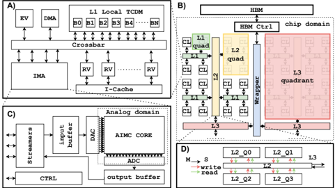
The image presents four technical diagrams (A-D) illustrating components of a computer architecture system. Each section depicts distinct subsystems with labeled blocks, directional arrows, and color-coded regions.
### Components/Axes
**Section A (Top-Left):**
- **EV (Event Buffer)**, **DMA (Direct Memory Access)**, **Local TCDM (Tile Cache Data Memory)**, **Crossbar**, **IMA (Instruction Memory Array)**, **I-Cache**, and **RVs (Registers)**.
- Arrows indicate data flow between blocks (e.g., EV → DMA → Local TCDM → Crossbar → IMA/I-Cache → RVs).
- Labels: B0-BN (Local TCDM banks), "Crossbar" (central horizontal block).
**Section B (Top-Right):**
- **HBM (High Bandwidth Memory)**, **HBM Ctrl (Controller)**, **Chip Domain**, and **Quadrants (L1, L2, L3)**.
- Color-coded regions: L1 (green), L2 (yellow), L3 (pink), Chip Domain (blue).
- Vertical "Wrapper" connects L2 and L3 quadrants.
**Section C (Bottom-Left):**
- **Analog Domain** components: **Streamers**, **Input Buffer**, **DAC (Digital-to-Analog Converter)**, **AIMC Core (Analog Integrated Mixed-signal Core)**, **ADC (Analog-to-Digital Converter)**, **Output Buffer**, and **CTRL (Control Unit)**.
- Arrows show signal flow: Streamers → Input Buffer → DAC → AIMC Core → ADC → Output Buffer.
**Section D (Bottom-Right):**
- **Timing Diagram** with **L2_Q0-Q3** (memory banks) and **M→S (Memory to System)** line.
- Red arrows (write) and green arrows (read) indicate operations between L2 and L3.
### Detailed Analysis
**Section A:**
- Local TCDM (B0-BN) feeds into Crossbar, which distributes data to IMA and I-Cache.
- RVs (Registers) receive data from I-Cache, suggesting a cache-to-register pipeline.
**Section B:**
- HBM is connected to HBM Ctrl, which interfaces with the Chip Domain.
- Quadrants L1-L3 are spatially separated, with L3 spanning the entire width.
**Section C:**
- Analog Domain processes signals sequentially: digital inputs (Streamers) → analog conversion (DAC) → core processing (AIMC) → digital output (ADC).
**Section D:**
- Write operations (red) target L2_Q0-Q1, while read operations (green) access L2_Q2-Q3, indicating partitioned memory access.
### Key Observations
- **Color Coding:** Sections B and D use color to differentiate functional units (e.g., L1-L3 quadrants, write/read operations).
- **Flow Direction:** Arrows in A and C indicate unidirectional data flow, while D shows bidirectional memory access.
- **Hierarchical Structure:** Section B’s quadrants suggest a multi-level memory hierarchy.
### Interpretation
The diagrams collectively represent a **heterogeneous computing architecture**:
1. **Section A** illustrates a **data processing pipeline** with local caching (TCDM) and crossbar arbitration.
2. **Section B** depicts a **3D chip layout** with HBM integration and quadrant-based memory organization.
3. **Section C** highlights **analog-digital signal processing**, emphasizing mixed-signal integration.
4. **Section D** shows **memory timing protocols**, with partitioned access patterns for write/read operations.
The system appears optimized for **high-performance computing**, combining parallel data processing (Crossbar), hierarchical memory (HBM quadrants), and analog-digital co-design. The timing diagram (D) suggests optimized memory access strategies to reduce latency.