## Circuit Diagrams: Analog Device Architectures
### Overview
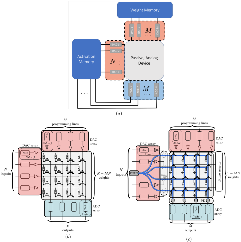
The image presents three circuit diagrams (a, b, c) illustrating different architectures for analog devices, likely used in machine learning or signal processing applications. Diagram (a) shows a high-level block diagram, while (b) and (c) depict more detailed circuit implementations.
### Components/Axes
**Diagram (a): High-Level Block Diagram**
* **Blocks:**
* Activation Memory (Blue rectangle, top-left)
* Passive, Analog Device (Gray rectangle, center)
* Weight Memory (Blue rectangle, top)
* DAC 1, DAC 2, ..., DAC K (Orange rectangles, left of Passive Analog Device)
* DAC 1, DAC 2, ..., DAC M (Gray rectangles, above Passive Analog Device)
* ADC 1, ADC 2, ..., ADC M (Blue rectangles, below Passive Analog Device)
* **Labels:**
* N (next to DAC K)
* M (next to DAC M and ADC M)
* **Connections:**
* Activation Memory connected to DACs (DAC 1 to DAC K)
* DACs (DAC 1 to DAC M) connected to Weight Memory
* DACs (DAC 1 to DAC K) connected to Passive, Analog Device
* Passive, Analog Device connected to ADCs (ADC 1 to ADC M)
* ADCs (ADC 1 to ADC M) connected back to Activation Memory
**Diagram (b): Detailed Circuit Implementation (First Architecture)**
* **Regions:**
* DAC array (Red rectangle, top-left)
* Labels: γdac, εdac,1, γdac, εdac,2
* ADC array (Blue rectangle, bottom)
* Labels: γadc, εadc
* Transistor Array (Gray rectangle, center)
* **Labels:**
* N inputs (left)
* M programming lines (top)
* M outputs (bottom)
* K = MN weights (right)
**Diagram (c): Detailed Circuit Implementation (Second Architecture)**
* **Regions:**
* DAC array (Red rectangle, top-left)
* Labels: γdac, εdac,1, γdac, εdac,2
* ADC array (Blue rectangle, bottom)
* Labels: γadc, εadc
* Bitline selector (Gray rectangle, center)
* **Labels:**
* N inputs (left)
* M programming lines (top)
* M outputs (bottom)
* K = MN weights (right)
* Source (Gray circle, left)
* VOA (Variable Optical Attenuator)
* PD (Photodiode)
* **Connections:**
* Input "source" splits into N paths, connected to the bitline selector.
* The bitline selector has connections to the ADC array.
### Detailed Analysis or ### Content Details
**Diagram (a):**
* The diagram shows a system with an Activation Memory providing inputs to a Passive, Analog Device.
* DACs (Digital-to-Analog Converters) are used to convert digital signals from the Activation Memory and Weight Memory into analog signals suitable for the Passive, Analog Device.
* ADCs (Analog-to-Digital Converters) convert the analog output of the Passive, Analog Device back into digital signals.
* The number of DACs connected to the Activation Memory is K, while the number of DACs/ADCs connected to the Passive, Analog Device is M.
**Diagram (b):**
* This diagram shows a circuit implementation using a DAC array, a transistor array, and an ADC array.
* The DAC array receives N inputs and generates analog signals that control the transistors in the transistor array.
* The transistor array performs a weighted sum of the inputs, with the weights determined by the programming lines.
* The ADC array converts the analog output of the transistor array into M digital outputs.
* The total number of weights is K = MN.
**Diagram (c):**
* This diagram shows an alternative circuit implementation using a DAC array, a bitline selector, and an ADC array.
* The DAC array receives N inputs from a "source" and generates analog signals that control the bitline selector.
* The bitline selector routes the analog signals to the ADC array based on the programming lines.
* The ADC array converts the analog signals into M digital outputs.
* The circuit includes Variable Optical Attenuators (VOA) and Photodiodes (PD).
* The total number of weights is K = MN.
### Key Observations
* Diagram (a) provides a high-level overview of the system architecture.
* Diagrams (b) and (c) present two different circuit implementations for the Passive, Analog Device.
* Both implementations use DACs and ADCs to interface between digital and analog domains.
* Diagram (c) utilizes optical components (VOA and PD) and a bitline selector, suggesting a different approach to signal processing compared to diagram (b).
### Interpretation
The diagrams illustrate different approaches to implementing analog devices for machine learning or signal processing. Diagram (a) sets the stage by showing the overall system architecture, highlighting the interaction between digital memory and an analog processing unit. Diagrams (b) and (c) then delve into specific circuit implementations. Diagram (b) uses a transistor array to perform weighted sums, while diagram (c) employs a bitline selector and optical components. The choice of implementation depends on factors such as performance requirements, power consumption, and area constraints. The use of optical components in diagram (c) suggests a potential for higher bandwidth and lower power consumption compared to the purely electronic implementation in diagram (b). The common goal is to efficiently perform analog computations, which can be advantageous for certain machine learning tasks.