## Diagram: Analog Neural Network Architecture
### Overview
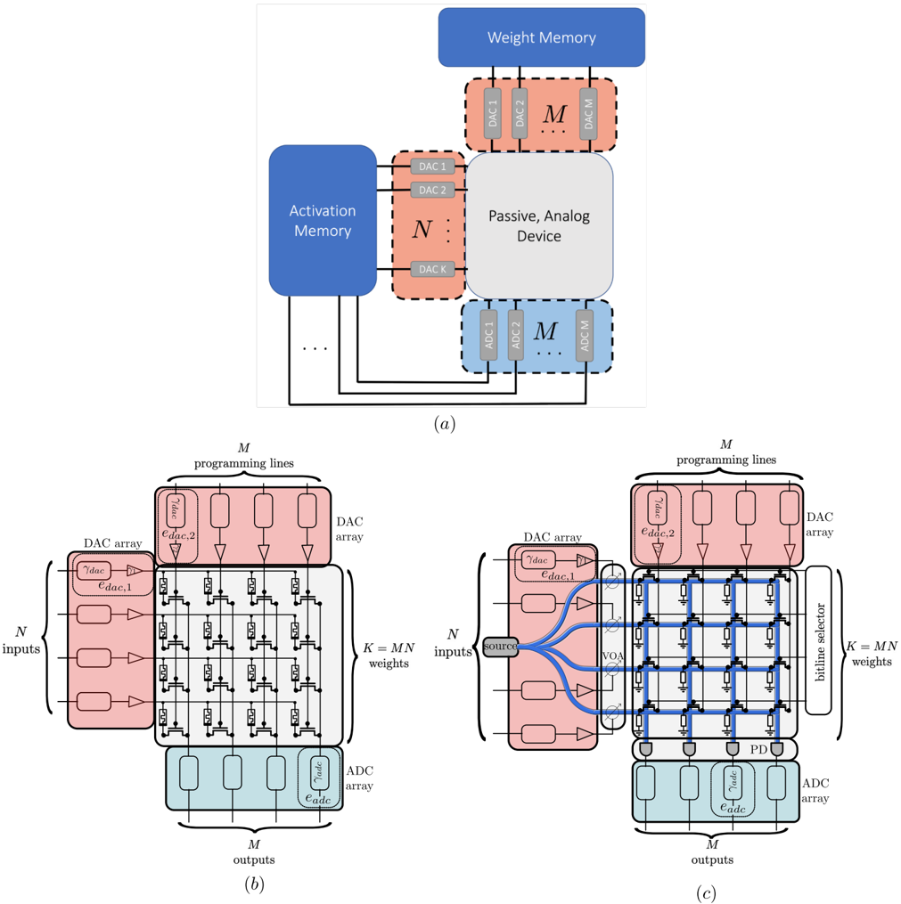
The image presents a schematic diagram illustrating the architecture of an analog neural network. It consists of three main sub-diagrams: (a) a high-level block diagram showing the overall system, (b) a detailed view of the Digital-to-Analog Converter (DAC) array and Analog-to-Digital Converter (ADC) array, and (c) a modified version of (b) incorporating a current source and bitline selector. The diagrams depict the flow of signals and the key components involved in implementing neural network computations in the analog domain.
### Components/Axes
The diagram features the following key components:
* **Weight Memory:** A rectangular block at the top, labeled "Weight Memory".
* **Activation Memory:** A rectangular block to the left, labeled "Activation Memory".
* **Passive, Analog Device:** A rectangular block in the center, labeled "Passive, Analog Device".
* **DAC Array:** Represented as a grid of smaller blocks labeled "DAC 1" through "DAC M" in diagram (a), and expanded in diagrams (b) and (c).
* **ADC Array:** Represented as a grid of smaller blocks labeled "ADC 1" through "ADC M" in diagram (a), and expanded in diagrams (b) and (c).
* **N Inputs:** Represented as input lines to the system.
* **M Outputs:** Represented as output lines from the system.
* **Programming Lines:** Horizontal lines connecting to the DAC array, labeled "M programming lines".
* **Bitline Selector:** A component in diagram (c) used to select bitlines.
* **Current Source:** A component in diagram (c) labeled "N source".
* **Voltage-to-Current Converter (V2A):** A component in diagram (c).
* **Pd:** A component in diagram (c).
* **εdac,1, εdac,2, εdac:** Labels indicating error sources within the DAC array.
* **εadc:** Label indicating error source within the ADC array.
* **τdac, τadc:** Labels indicating time constants within the DAC and ADC arrays.
### Detailed Analysis or Content Details
**Diagram (a): System Overview**
* The "Weight Memory" is connected to the "Passive, Analog Device" via "M" DACs (DAC 1 to DAC M).
* The "Activation Memory" is connected to the "Passive, Analog Device" via "N" inputs.
* The "Passive, Analog Device" outputs "M" signals through "M" ADCs (ADC 1 to ADC M).
* The diagram shows a bidirectional connection between the "Activation Memory" and the "Passive, Analog Device" using dotted lines.
**Diagram (b): DAC/ADC Array Details**
* The DAC array consists of a grid of cells. Each cell contains a programming line input, a capacitor labeled "εdac,1" and "εdac,2", and a switch.
* The ADC array consists of a grid of cells. Each cell contains a capacitor labeled "εadc" and a switch.
* There are "N" inputs to the DAC array and "M" outputs from the ADC array.
* The diagram shows "M" programming lines controlling the DAC array.
**Diagram (c): Modified DAC/ADC Array with Current Source and Bitline Selector**
* This diagram is similar to (b) but includes a current source labeled "N source" connected to the DAC array.
* A Voltage-to-Current Converter (V2A) is present.
* A bitline selector is used to control the output of the ADC array.
* A component labeled "Pd" is included.
### Key Observations
* The diagrams illustrate a mixed-signal approach to neural network implementation, combining digital memory (Weight and Activation Memory) with analog computation (Passive, Analog Device).
* The use of DACs and ADCs suggests that the neural network operates by converting digital weights and activations into analog signals for computation and then converting the results back to digital form.
* The inclusion of error sources (εdac,1, εdac,2, εdac) indicates that the designers are considering the impact of analog imperfections on the network's performance.
* The addition of the current source and bitline selector in diagram (c) suggests an optimization or alternative implementation of the DAC/ADC array.
### Interpretation
The diagrams depict a potential architecture for building analog neural networks. The core idea is to leverage the inherent parallelism and energy efficiency of analog circuits to accelerate neural network computations. The Weight Memory stores the synaptic weights, while the Activation Memory stores the neuron activations. The Passive, Analog Device performs the weighted sum and non-linear activation functions in the analog domain. The DACs and ADCs serve as interfaces between the digital and analog worlds.
The inclusion of error sources highlights the challenges of building accurate and reliable analog circuits. Analog imperfections can introduce noise and errors into the computation, which can degrade the network's performance. The designers are likely exploring techniques to mitigate these errors, such as calibration or error correction.
The modified architecture in diagram (c) suggests an attempt to improve the performance or efficiency of the DAC/ADC array. The current source and bitline selector may be used to optimize the signal-to-noise ratio or reduce power consumption.
Overall, the diagrams provide a glimpse into the design considerations and trade-offs involved in building analog neural networks. This approach holds promise for achieving significant performance and energy efficiency gains compared to traditional digital implementations, but it also presents significant challenges in terms of accuracy, reliability, and scalability. The diagrams are a technical illustration of a potential solution, rather than a presentation of data.