## Circuit Diagram with Timing Charts
### Overview
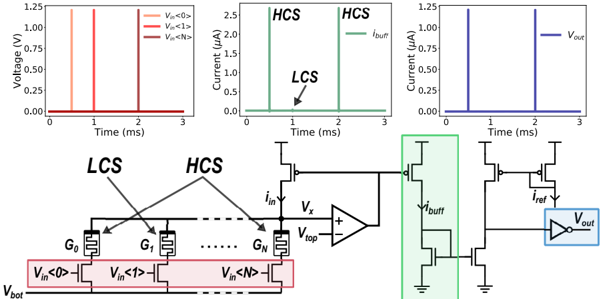
The image presents a circuit diagram coupled with three timing charts illustrating the voltage and current behavior at different points in the circuit. The circuit involves memristors, transistors, and an operational amplifier, ultimately producing an output voltage. The timing charts show the input voltage pulses, buffer current, and output voltage over time.
### Components/Axes
**Timing Charts (Top Row):**
* **X-axis (all charts):** Time (ms), ranging from 0 to 3 ms.
* **Top-Left Chart:**
* Y-axis: Voltage (V), ranging from 0 to 1.25 V.
* Data Series:
* `Vin<0>`: Light orange pulses at approximately 0.5 ms.
* `Vin<1>`: Red pulses at approximately 1.5 ms.
* `Vin<N>`: Dark red pulses at approximately 2.5 ms.
* **Top-Middle Chart:**
* Y-axis: Current (μA), ranging from 0 to 2.5 μA.
* Data Series:
* `Ibuff`: Green pulses at approximately 1 ms and 2 ms.
* Annotations: "HCS" (High Conductance State) above the pulses, "LCS" (Low Conductance State) below the first pulse.
* **Top-Right Chart:**
* Y-axis: Current (μA), ranging from 0 to 1.25 μA.
* Data Series:
* `Vout`: Blue pulses at approximately 2 ms.
**Circuit Diagram (Bottom):**
* **Memristor Array:** Labeled `G0`, `G1`, ..., `GN`. Connected to input voltages `Vin<0>`, `Vin<1>`, ..., `Vin<N>`.
* **Input Voltages:** `Vin<0>`, `Vin<1>`, `Vin<N>` are connected to transistors.
* **Operational Amplifier:** Labeled with "+" and "-". Inputs are `Vx` and `Vtop`.
* **Buffer Stage:** Enclosed in a green box, labeled `Ibuff`.
* **Output Stage:** Enclosed in a blue box, labeled `Vout`.
* **Currents:** `Iin` and `Iref` are labeled.
* **Voltage:** `Vbot` is labeled.
### Detailed Analysis or Content Details
**Timing Charts:**
* **`Vin<0>`:** A voltage pulse of approximately 1.25V at around 0.5 ms.
* **`Vin<1>`:** A voltage pulse of approximately 1.25V at around 1.5 ms.
* **`Vin<N>`:** A voltage pulse of approximately 1.25V at around 2.5 ms.
* **`Ibuff`:** Current pulses of approximately 2.25 μA at around 1 ms and 2 ms.
* **`Vout`:** A current pulse of approximately 1.25 μA at around 2 ms.
**Circuit Diagram:**
* The memristor array is connected to input voltages via transistors.
* The output of the memristor array feeds into an operational amplifier.
* The operational amplifier's output drives a buffer stage.
* The buffer stage's output drives the final output stage, producing `Vout`.
### Key Observations
* The input voltage pulses (`Vin<0>`, `Vin<1>`, `Vin<N>`) occur at different times.
* The buffer current (`Ibuff`) pulses correspond to the input voltage pulses.
* The output voltage (`Vout`) pulse occurs after the buffer current pulse.
* The annotations "HCS" and "LCS" indicate the high and low conductance states of the memristors.
### Interpretation
The diagram illustrates a circuit that uses memristors as input elements. The input voltages control the conductance of the memristors, which in turn affects the current flowing through the circuit. The operational amplifier and buffer stage amplify and shape the signal before it reaches the output. The timing charts show how the voltage and current change at different points in the circuit over time. The "HCS" and "LCS" annotations suggest that the memristors are switching between high and low conductance states, which is a key characteristic of memristor behavior. The circuit appears to be implementing a logic function or signal processing operation based on the memristor array.