## Circuit System Response Analysis
### Overview
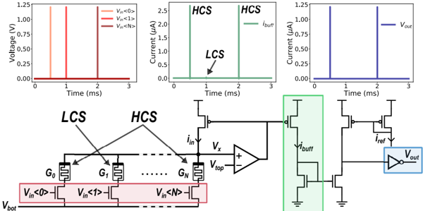
The image presents a technical analysis of a circuit system's response to input voltage thresholds, featuring three time-domain graphs and a circuit diagram. The graphs depict voltage/current responses over time (0-3ms) for different input conditions, while the circuit diagram illustrates component relationships and signal flow.
### Components/Axes
**Graph 1 (Left):**
- **X-axis**: Time (ms) [0, 1, 2, 3]
- **Y-axis**: Voltage (V) [0.0, 0.25, 0.5, 0.75, 1.0, 1.25]
- **Legend**:
- Orange: V_in <0> (top-left)
- Red: V_in <1> (middle)
- Dark Red: V_in <N> (bottom)
- **Key Elements**: Vertical voltage spikes at specific time points
**Graph 2 (Center):**
- **X-axis**: Time (ms) [0, 1, 2, 3]
- **Y-axis**: Current (μA) [0, 0.5, 1.0, 1.5, 2.0, 2.5]
- **Legend**:
- Green: HCS (right)
- Green Arrow: LCS (pointing to 2ms spike)
- **Key Elements**: Current spikes at 1ms (HCS) and 2ms (LCS)
**Graph 3 (Right):**
- **X-axis**: Time (ms) [0, 1, 2, 3]
- **Y-axis**: Current (μA) [0, 0.25, 0.5, 0.75, 1.0]
- **Legend**:
- Blue: V_out (right)
- **Key Elements**: Current spike at 3ms
**Circuit Diagram (Bottom):**
- **Components**:
- G0, G1, ..., GN (voltage-controlled switches)
- V_bot (input voltage source)
- V_in (input voltage thresholds)
- V_x (intermediate voltage)
- V_top (reference voltage)
- i_in, i_buff, i_ref (current paths)
- V_out (output voltage)
- **Signal Flow**:
- Input voltages (V_in) trigger G0-GN switches
- Current paths split between HCS (i_buff) and LCS (i_ref)
- Output V_out generated through operational amplifier
### Detailed Analysis
**Graph 1 Trends:**
- V_in <0> (orange): 1.2V spike at 1ms
- V_in <1> (red): 1.0V spike at 2ms
- V_in <N> (dark red): 0.8V spike at 3ms
- All spikes show 0V baseline before/after events
**Graph 2 Trends:**
- HCS (green): 2.5μA spike at 1ms (duration ~1ms)
- LCS (green): 1.5μA spike at 2ms (duration ~1ms)
- No overlap between HCS and LCS current paths
**Graph 3 Trends:**
- V_out (blue): 1.0μA spike at 3ms (duration ~1ms)
- No activity before 3ms
**Circuit Diagram Details:**
- Voltage thresholds (V_in <0>, <1>, <N>) control G0-GN switches
- HCS path: V_x → i_buff → V_out
- LCS path: V_top → i_ref → V_out
- Operational amplifier configuration suggests current summation
### Key Observations
1. Voltage response precedes current response by 1ms (Graph 1 spikes at 1ms precede Graph 2 HCS at 1ms)
2. LCS response delayed by 1ms compared to HCS (2ms vs 1ms)
3. Output current (V_out) delayed by 1ms compared to LCS (3ms vs 2ms)
4. Current magnitudes decrease with increasing input threshold (2.5→1.5→1.0μA)
### Interpretation
This system demonstrates a cascaded response mechanism where:
1. Input voltage thresholds (V_in) trigger sequential activation of G0-GN switches
2. HCS (High Current Switch) responds first at 1ms, followed by LCS (Low Current Switch) at 2ms
3. Output current (V_out) integrates both paths with a 1ms delay, suggesting processing time
4. Current magnitude inversely correlates with input threshold sensitivity (higher thresholds = lower currents)
The circuit appears to implement a time-multiplexed current switching system with threshold-dependent response characteristics. The 1ms delays between stages suggest intentional design for sequential processing, while the current magnitude differences indicate varying load capacities for different input conditions.