## Circuit Diagram: Analog In-Memory Computing (AIMC) Architecture
### Overview
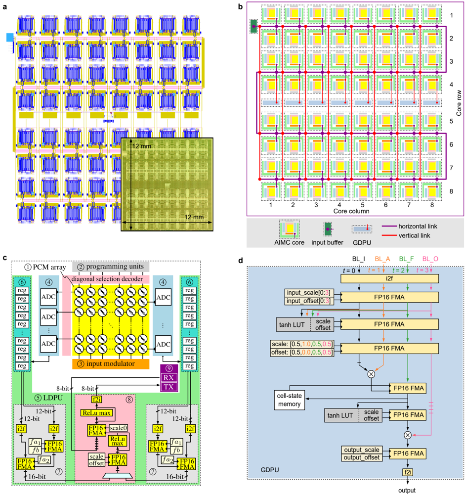
The image presents a detailed circuit diagram of an Analog In-Memory Computing (AIMC) architecture. It comprises several interconnected components, including an array of AIMC cores, input buffers, GDPUs (General-purpose Digital Processing Units), PCM (Phase Change Memory) arrays, and other processing units. The diagram is divided into four sub-figures (a, b, c, d), each illustrating different aspects of the architecture.
### Components/Axes
**Sub-figure a:**
* Shows a high-level layout of the AIMC cores.
* Includes a zoomed-in section with dimensions of 12 mm x 12 mm.
**Sub-figure b:**
* Illustrates the arrangement of AIMC cores in an 8x8 grid.
* Labels the core rows and columns from 1 to 8.
* Legend:
* AIMC core (light green)
* Input buffer (dark green)
* GDPU (light blue)
* Horizontal link (purple)
* Vertical link (red)
**Sub-figure c:**
* Presents a detailed block diagram of the processing units.
* Key components:
* PCM array (labeled ①)
* Programming units (labeled ②)
* Input modulator (labeled ③)
* ADCs (Analog-to-Digital Converters, labeled ④)
* LDPU (Local Digital Processing Unit, labeled ⑤)
* Registers (labeled ⑥)
* FP16 FMA blocks (labeled ⑦)
* ReLU max blocks (labeled ⑧)
* RX/TX (Receiver/Transmitter, labeled ⑨)
* Data paths are labeled with bit widths (8-bit, 12-bit, 16-bit).
**Sub-figure d:**
* Shows the architecture of a GDPU.
* Key components:
* Input scale/offset blocks
* tanh LUT (Look-Up Table)
* FP16 FMA blocks
* Cell-state memory
* Output scale/offset blocks
* Signals are labeled as BL_I, BL_A, BL_F, BL_O, representing different stages of processing.
* Time steps are indicated as t=0, t=1, t=2, t=3.
* Specific scale and offset values are provided:
* scale: [0.5, 1.0, 0.5, 0.5]
* offset: [0.5, 0.0, 0.5, 0.5]
### Detailed Analysis or ### Content Details
**Sub-figure a:**
* The AIMC cores are arranged in a grid-like structure.
* The zoomed-in section shows the detailed layout of the core.
**Sub-figure b:**
* The 8x8 grid of AIMC cores is interconnected via horizontal (purple) and vertical (red) links.
* Each AIMC core is surrounded by an input buffer (dark green) and a GDPU (light blue).
**Sub-figure c:**
* The PCM array is connected to the programming units via a diagonal selection decoder.
* The input modulator processes the input signals before they are fed into the LDPU.
* The LDPU performs digital processing on the data, including FP16 FMA operations and ReLU max activation.
* The RX/TX block handles communication with other parts of the system.
**Sub-figure d:**
* The GDPU performs a series of operations, including scaling, offsetting, tanh activation, and FP16 FMA.
* The cell-state memory stores intermediate results.
* The output is generated after several processing stages.
### Key Observations
* The AIMC architecture integrates analog and digital processing units.
* The 8x8 grid structure allows for parallel processing.
* The GDPU architecture is designed for efficient computation of neural network operations.
* The use of FP16 FMA blocks enables high-performance floating-point arithmetic.
### Interpretation
The AIMC architecture is designed to accelerate neural network computations by performing analog in-memory computing. The integration of PCM arrays, ADCs, and GDPUs allows for efficient data storage, conversion, and processing. The 8x8 grid structure enables parallel processing, which can significantly improve performance. The GDPU architecture is optimized for neural network operations, such as matrix multiplication and activation functions. The use of FP16 FMA blocks provides a good balance between precision and performance. The specific scale and offset values in the GDPU suggest that the architecture is designed for a specific type of neural network or application.