## Diagram: Analog In-Memory Computing (AIMC) Architecture
### Overview
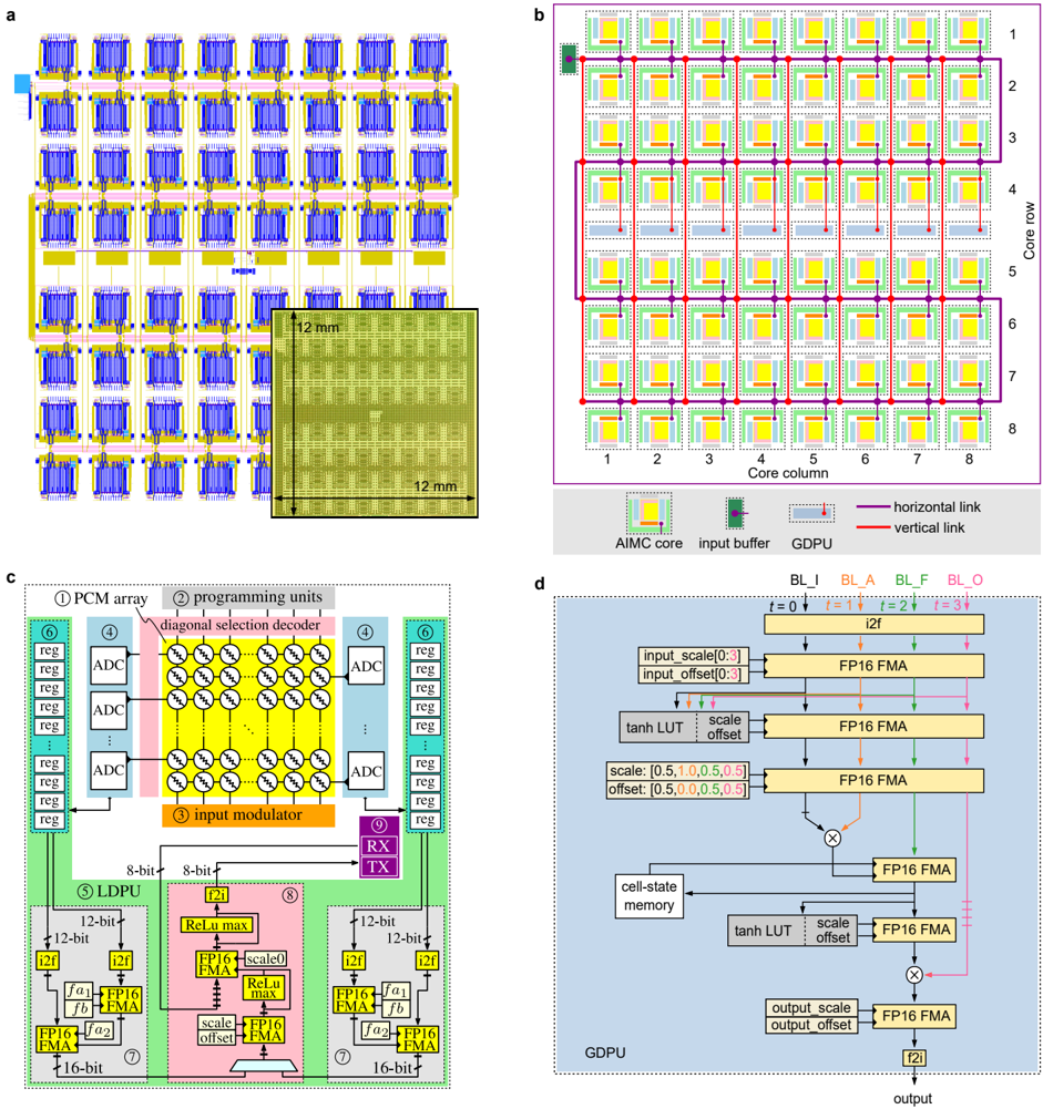
The image presents a detailed schematic of an Analog In-Memory Computing (AIMC) architecture. It comprises four distinct sections: (a) a photograph of the physical chip, (b) a layout of the core array, (c) a block diagram of the PCM array and programming units, and (d) a detailed flow diagram of the GDPU (Grainy Digital Processing Unit). The diagram illustrates the hardware components and data flow within an AIMC system, focusing on the integration of phase-change memory (PCM) for analog computation.
### Components/Axes
* **(a) Physical Chip:** Shows a rectangular chip with a grid-like pattern of metallic pads. Scale bar indicates 12 mm.
* **(b) Core Array Layout:** A grid of 8x8 cores, labeled with core row (1-8) and core column (1-8) axes. Cores are color-coded: green, yellow, and red. Horizontal and vertical link indicators are present.
* **(c) PCM Array & Programming Units:** Block diagram with labeled components: PCM array, diagonal selection decoder, input modulator, ADC (Analog-to-Digital Converter), registers (reg), and GDPU. Data flow is indicated by arrows and bit widths (8-bit, 12-bit, 16-bit).
* **(d) GDPU Flow Diagram:** Detailed flow of data through the GDPU, including input scaling, tanh LUT (Look-Up Table), cell-state memory, and FP16 FMA (Fused Multiply-Add) operations. Control signals (BL_I, BL_A, BL_F, BL_O) are indicated.
### Detailed Analysis or Content Details
**(a) Physical Chip:**
The image shows a physical chip with a regular array of connection pads. The dimensions are approximately 12mm x 12mm. The chip appears to be fabricated with metallic interconnects.
**(b) Core Array Layout:**
The core array consists of 64 cores arranged in an 8x8 grid.
* **Color Coding:**
* Green cores: Appear to be the majority, distributed throughout the array.
* Yellow cores: Scattered throughout the array.
* Red cores: Fewer in number, also scattered.
* **Links:** Horizontal and vertical links connect adjacent cores, facilitating data communication.
**(c) PCM Array & Programming Units:**
* **PCM Array:** Contains multiple PCM cells connected to ADCs and registers. The diagram shows a repeating structure of PCM cells, ADCs, and registers.
* **Diagonal Selection Decoder:** Selects diagonal elements within the PCM array.
* **Input Modulator:** Modulates the input signal.
* **ADC:** Converts analog signals to digital.
* **Registers (reg):** Store digital values.
* **GDPU:** Receives data from the PCM array and performs further processing.
* **Data Flow:**
* Input signal goes through the input modulator.
* The modulated signal is processed by the PCM array.
* The output of the PCM array is converted to digital by the ADC.
* The digital signal is stored in registers and sent to the GDPU.
* The GDPU performs operations like ReLU max and scaled FP16 FMA.
* **Bit Widths:**
* Input to GDPU: 8-bit
* Intermediate processing: 12-bit
* Output of GDPU: 16-bit
**(d) GDPU Flow Diagram:**
* **Input Scaling:** Input signal is scaled using a scale factor [0:3] and offset [0:3].
* **Tanh LUT:** The scaled input is passed through a hyperbolic tangent Look-Up Table (tanh LUT).
* **Cell-State Memory:** Stores the cell state.
* **FP16 FMA:** Multiple FP16 Fused Multiply-Add operations are performed.
* **Output Scaling:** The output is scaled using a scale factor [0:5, 0:0, 0:5, 0:5] and offset [0:5, 0:0, 0:5, 0:5].
* **Control Signals:** BL_I, BL_A, BL_F, BL_O are control signals for the memory cells.
### Key Observations
* The AIMC architecture integrates analog computation within the memory array using PCM cells.
* The GDPU provides digital processing capabilities to complement the analog computation.
* The use of FP16 FMA operations suggests a focus on efficient and accurate computation.
* The core array layout with different colored cores may indicate different functionalities or configurations.
* The diagram highlights the importance of scaling and offset adjustments for accurate analog computation.
### Interpretation
The diagram illustrates a novel AIMC architecture that leverages the inherent parallelism of memory arrays for efficient computation. By performing computations directly within the memory, the architecture reduces data movement and energy consumption compared to traditional von Neumann architectures. The integration of PCM cells enables analog computation, while the GDPU provides digital processing capabilities for control and post-processing. The use of FP16 FMA operations suggests a focus on achieving high accuracy and performance. The color-coded core array layout may indicate a heterogeneous architecture where different cores are optimized for different tasks. The scaling and offset adjustments are crucial for mitigating variations in PCM cell characteristics and ensuring accurate computation. This architecture is likely targeted towards applications requiring high energy efficiency and low latency, such as edge computing and machine learning. The diagram suggests a complex system with careful consideration given to both analog and digital components, and their interplay.