TECHNICAL ASSET FINGERPRINT
6ad274d8364b49935d88cf75
Click to view fullscreen
Press ESC or click to close
FOUND IN PAPERS
EXPERT: healer-alpha-free VERSION 1
RUNTIME: free/openrouter/healer-alpha
INTEL_VERIFIED
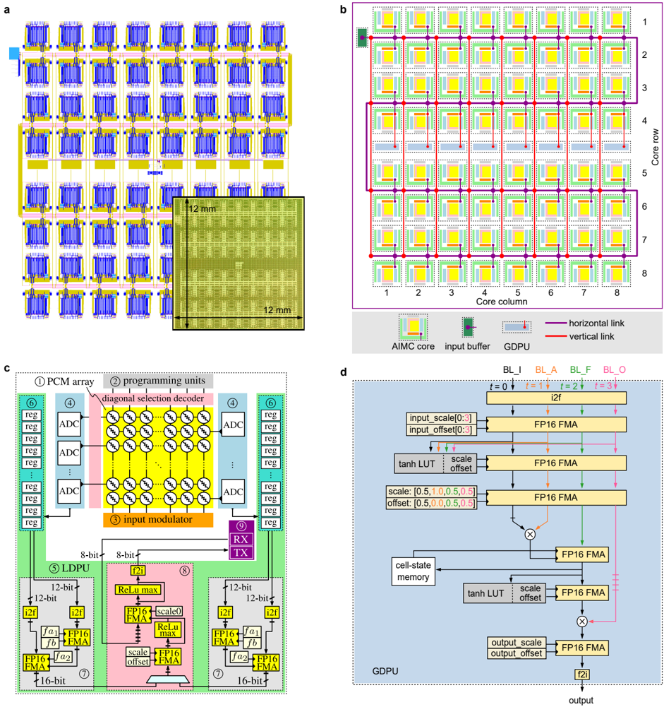
## Technical Diagram: AI Memory Computing (AIMC) Core Architecture and Chip Layout
### Overview
The image is a composite technical figure containing four distinct panels (a, b, c, d) that collectively describe the physical layout, core array organization, internal block diagram, and data processing flow of an Analog In-Memory Computing (AIMC) system, likely designed for neural network acceleration. The language is English.
### Components/Axes
**Panel a: Physical Chip Layout**
* **Main Element:** A large grid of repeating blue and yellow rectangular units, representing the physical layout of AIMC cores on a chip.
* **Inset Photograph:** A micrograph of the fabricated chip die.
* **Labels/Annotations:**
* A scale bar within the main grid labeled "1 mm".
* Dimensions on the inset photograph: "12 mm" (height) and "12 mm" (width), indicating the chip die size is 12mm x 12mm.
**Panel b: Core Array Schematic**
* **Main Element:** An 8x8 grid of squares representing AIMC cores.
* **Axes:**
* **Vertical Axis (Left):** Labeled "Core row", numbered 1 through 8 from top to bottom.
* **Horizontal Axis (Bottom):** Labeled "Core column", numbered 1 through 8 from left to right.
* **Legend (Bottom Right):**
* **Symbol:** A yellow square with a green border. **Label:** "AIMC core".
* **Symbol:** A small green rectangle with a black border. **Label:** "input buffer".
* **Symbol:** A small red rectangle with a black border. **Label:** "GDPU" (General Digital Processing Unit).
* **Line (Purple):** **Label:** "horizontal link".
* **Line (Red):** **Label:** "vertical link".
* **Spatial Grounding:** The legend is positioned in the bottom-right corner of the panel. The purple horizontal links connect cores within the same row. The red vertical links connect cores within the same column.
**Panel c: AIMC Core Block Diagram**
* **Main Element:** A detailed schematic of a single AIMC core, divided into colored functional blocks with numbered labels.
* **Numbered Components (1-9):**
1. **PCM array:** A central yellow grid of circles (representing Phase-Change Memory cells).
2. **programming units:** Located above the PCM array.
3. **input modulator:** An orange block below the PCM array.
4. **ADC:** Analog-to-Digital Converters (blue blocks on left and right sides).
5. **LDPU:** Local Digital Processing Unit (green block on the left).
6. **reg:** Registers (stacked green boxes on the far left and right).
7. **FP16 FMA:** Floating-Point 16 Multiply-Accumulate units (yellow boxes within the LDPU and GDPU).
8. **GDPU:** General Digital Processing Unit (pink block in the center-bottom).
9. **RX/TX:** Receiver/Transmitter (purple block on the right).
* **Data Path Labels:**
* "8-bit" (arrows between ADC and LDPU/GDPU).
* "12-bit" (arrows within LDPU/GDPU).
* "16-bit" (output arrows from LDPU/GDPU).
* "i2f" (integer-to-float converters).
* "ReLU max" (activation function blocks).
* "scale", "offset" (parameters for normalization).
**Panel d: GDPU Data Flow Diagram**
* **Main Element:** A flowchart detailing the operations within the General Digital Processing Unit (GDPU).
* **Input/Output Labels (Top):**
* `BL_I`, `BL_A`, `BL_F`, `BL_O` (likely different bit-line or data types).
* `t = 0`, `t = 1`, `t = 2`, `t = 3` (indicating time steps or pipeline stages).
* **Processing Blocks:**
* `i2f` (integer to float).
* `FP16 FMA` (Floating-Point 16 Multiply-Accumulate) - appears multiple times.
* `tanh LUT` (Look-Up Table for hyperbolic tangent activation).
* `cell-state memory`.
* Multiplication nodes (circles with '×').
* **Parameter Labels:**
* `input_scale[0:3]`, `input_offset[0:3]`.
* `scale: [0.5, 1.0, 0.5, 0.5]`, `offset: [0.5, 0.0, 0.5, 0.5]`.
* `output_scale`, `output_offset`.
* **Final Output:** An arrow labeled "output" at the bottom.
### Detailed Analysis
* **Panel a:** Shows a highly regular, tiled architecture. The 12mm x 12mm chip contains a large array of identical AIMC core tiles, each approximately 1mm in scale based on the inset scale bar.
* **Panel b:** Defines the network topology. The 8x8 core array is interconnected via a mesh network of horizontal (purple) and vertical (red) links. Each core (yellow) has an associated input buffer (green) and a GDPU (red). The data flow appears to be systolic or wavefront-based, moving along the links.
* **Panel c:** Details the internal architecture of one core. The core performs analog computing using a PCM array (1). Analog inputs are modulated (3), processed by the memory array, and converted to digital via ADCs (4). Digital processing is handled by two specialized units: the LDPU (5) for lower-precision tasks and the GDPU (8) for higher-precision, sequential operations (like those in RNNs/LSTMs, suggested by the `tanh LUT` and `cell-state` in panel d). Data moves between units at 8-bit, 12-bit, and 16-bit precision.
* **Panel d:** Illustrates a specific data pipeline within the GDPU, likely for a recurrent neural network cell (e.g., LSTM or GRU). It shows a sequence of operations over four time steps (`t=0` to `t=3`), involving scaling, offset application, FMA operations, activation functions (`tanh LUT`), and multiplication, with state being stored in "cell-state memory".
### Key Observations
1. **Hierarchical Design:** The system is organized hierarchically: Chip (a) -> Core Array (b) -> Single Core (c) -> Digital Processing Unit (d).
2. **Analog-Digital Hybrid:** The core (c) combines analog in-memory computing (PCM array) with significant digital post-processing (LDPU, GDPU).
3. **Precision Scaling:** Data precision increases as it moves through the pipeline: from analog, to 8-bit digital after ADC, to 12-bit and 16-bit within the digital processing units.
4. **Specialized Processors:** The core contains two distinct digital processors (LDPU and GDPU), suggesting a division of labor between simple, parallel operations and complex, sequential operations.
5. **Recurrent Network Support:** The GDPU data flow (d) with `cell-state memory` and time steps (`t`) is explicitly designed for processing sequential data, characteristic of Recurrent Neural Networks (RNNs).
### Interpretation
This figure describes a specialized hardware accelerator for artificial intelligence, specifically targeting neural network inference. The architecture addresses the "memory wall" problem by performing computations directly within the memory array (the PCM array in panel c), which is highly energy-efficient for matrix-vector multiplication operations fundamental to AI.
The design emphasizes scalability (8x8 core array), precision management for accuracy, and flexibility to handle both feed-forward and recurrent network layers. The inclusion of a GDPU with a defined pipeline for recurrent operations indicates this chip is designed for complex tasks like natural language processing or time-series analysis, not just simple image classification. The 12mm x 12mm die size suggests a balance between computational throughput and manufacturing cost. The entire system represents a move away from traditional von Neumann architectures towards more efficient, domain-specific computing hardware for AI.
DECODING INTELLIGENCE...