## Diagram: Integrated Circuit Architecture and Data Flow
### Overview
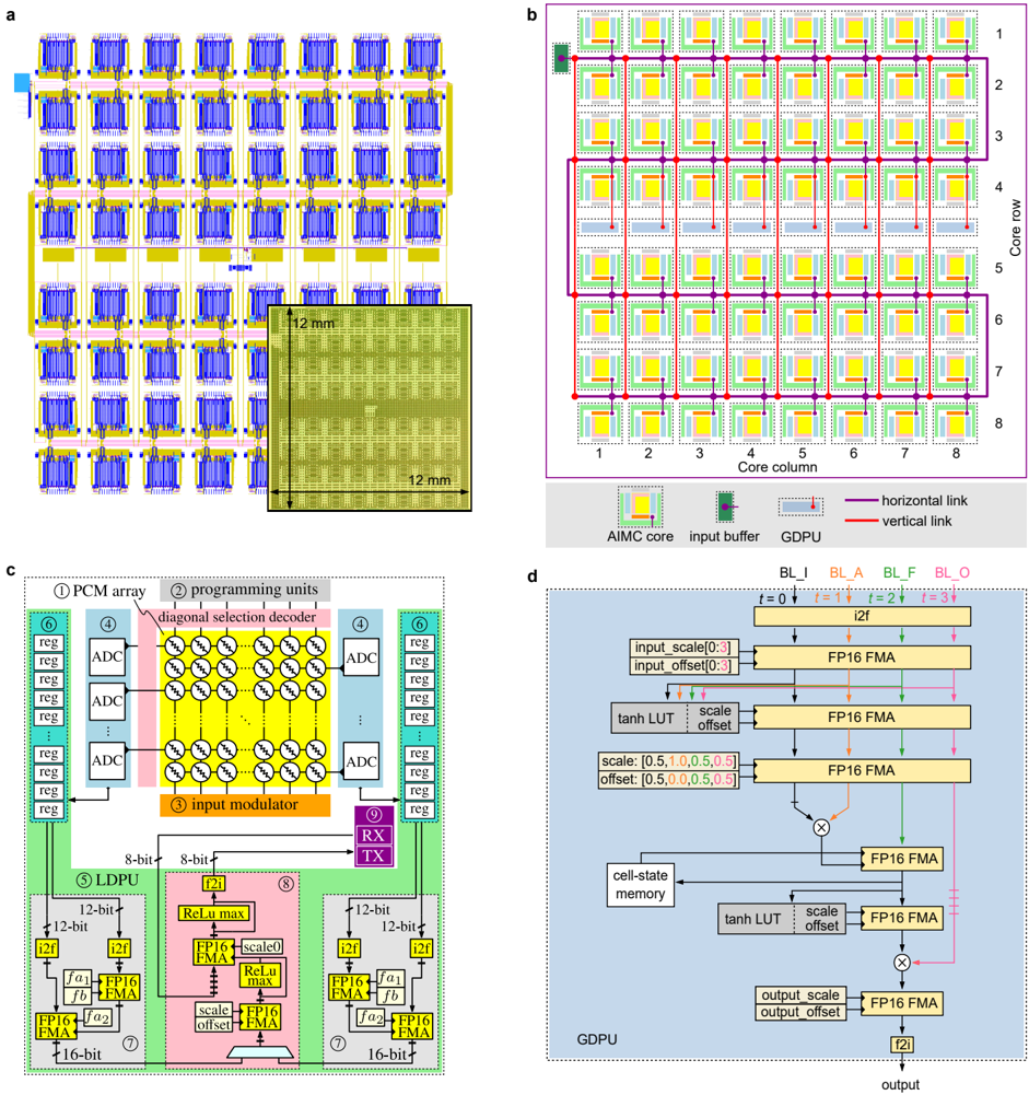
The image presents four technical diagrams illustrating an integrated circuit (IC) architecture, including component layout, connectivity, and data processing flow. Sections a-d depict physical layout, grid organization, block-level architecture, and computational workflow.
### Components/Axes
#### Section a: Physical Layout
- **Grid Structure**: 64 blue/yellow components arranged in 8x8 grid (rows 1-8, columns 1-8)
- **Scale Bar**: 12mm x 12mm reference in bottom-right corner
- **Legend**:
- Blue: AIME core
- Yellow: Input buffer
- Red: GDPU
- **Positioning**:
- Legend: Bottom-right of grid
- Scale bar: Overlapping bottom-right corner
#### Section b: Grid Organization
- **Axes**:
- X-axis: Core columns (1-8)
- Y-axis: Core rows (1-8)
- **Legend**:
- Purple: Horizontal links
- Red: Vertical links
- Blue: Input buffer
- Yellow: GDPU
- Green: AIME core
- **Positioning**:
- Legend: Bottom of diagram
- Axes labels: Along grid edges
#### Section c: Block Diagram
- **Components**:
1. PCM array (top-left)
2. Programming units (center)
3. Diagonal selection decoder (center-right)
4. Input modulator (bottom-center)
5. LDU (bottom-left)
6. RX/TX blocks (right)
- **Legend**:
- Yellow: PCM array
- Pink: Programming units
- Blue: ADC blocks
- Purple: RX/TX
- Green: LDU
- **Positioning**:
- Legend: Bottom of diagram
- Arrows indicate data flow direction
#### Section d: Computational Flow
- **Blocks**:
- FP16 FMA (repeated 5x)
- Tanh LUT
- Scale/offset operations
- Memory blocks
- **Legend**:
- Green: BL_I/BL_A/BL_F/BL_O
- Purple: FP16 FMA
- Gray: Tanh LUT
- Blue: Scale/offset
- **Positioning**:
- Legend: Bottom-left
- Flow direction: Top-to-bottom
### Detailed Analysis
#### Section a
- Components form a regular 8x8 matrix with alternating blue (AIME core) and yellow (input buffer) elements
- GDPU elements (red) form perimeter around grid
- Scale bar confirms physical dimensions (12mm x 12mm)
#### Section b
- Grid shows connectivity pattern:
- Horizontal links (purple) connect adjacent columns
- Vertical links (red) connect adjacent rows
- Input buffers (blue) and GDPUs (yellow) form boundary elements
#### Section c
- Data flow path:
1. PCM array → Programming units → Diagonal decoder → Input modulator
2. Parallel processing through LDU and RX/TX blocks
- 8-bit/12-bit/16-bit data paths indicated
#### Section d
- Computational pipeline:
1. Input scaling (0.3) → FP16 FMA
2. Tanh activation → Scale/offset operations
3. Memory access → Final output scaling
- 16-bit output path confirmed
### Key Observations
1. Regular grid structure suggests parallel processing capabilities
2. Perimeter GDPU elements likely handle input/output management
3. FP16 FMA blocks dominate computational path (5 instances)
4. Scale/offset operations appear at multiple pipeline stages
5. Tanh activation function indicates non-linear processing
### Interpretation
This architecture combines:
- **Physical Layout**: Dense matrix of processing elements (A) with peripheral I/O (GDPU)
- **Connectivity**: Regular grid interconnects (B) enabling efficient data sharing
- **Computation**: Multi-stage processing pipeline (D) with specialized units (C)
- **Memory**: Integrated PCM array (C) for non-volatile storage
The design emphasizes:
1. High-density parallel processing (8x8 core array)
2. Low-latency data flow (direct interconnects between cores)
3. Mixed-precision computation (FP16/FMA with 8/12/16-bit paths)
4. Energy-efficient memory access (PCM array integration)
Notable design choices include:
- Use of tanh activation for non-linearity
- Multiple scale/offset operations for dynamic range control
- Peripheral GDPU elements for I/O buffering
- Diagonal selection decoder for optimized data routing