## Block Diagrams: FFLUT, hFFLUT, and LUT Generator
### Overview
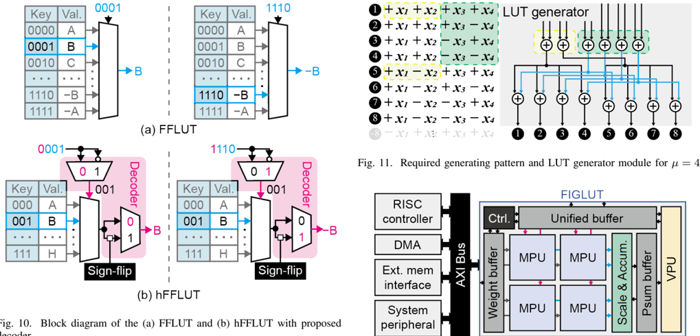
The image contains three technical diagrams:
1. **(a) FFLUT**: A data processing block diagram with key-value tables, a decoder, and sign-flip logic.
2. **(b) hFFLUT**: Similar to FFLUT but includes a decoder with explicit sign-flip components.
3. **LUT Generator**: A module for generating address patterns with arithmetic operations on variables.
4. **FIGLUT**: A system architecture diagram integrating RISC controllers, memory units, and processing pipelines.
---
### Components/Axes
#### (a) FFLUT
- **Left Table**:
- **Columns**: `Key` (4-bit binary), `Val` (alphanumeric).
- **Rows**:
- `0000` → `A`
- `0001` → `B` (highlighted in blue)
- `0010` → `C`
- `1110` → `B`
- `1111` → `-A`
- **Arrow**: Blue arrow from `0001` (B) to `1110` (-B).
- **Right Table**:
- **Columns**: `Key` (4-bit binary), `Val` (alphanumeric).
- **Rows**:
- `0000` → `A`
- `0001` → `B`
- `0010` → `C`
- `1110` → `-B` (highlighted in blue)
- `1111` → `-A`
- **Decoder**:
- Input: `0 1` (binary)
- Output: `0` or `1`
- **Sign-flip**: Labeled "Sign-flip" in black box.
#### (b) hFFLUT
- **Decoder**:
- Input: `0 1` (binary)
- Output: `0` or `1`
- **Sign-flip**: Explicitly labeled "Sign-flip" in black box.
#### LUT Generator (Fig 11)
- **Generating Pattern**:
- Equations for 8 outputs (1–8):
- `1`: `1 + x1 + x2 + x3 + x4`
- `2`: `2 + x1 + x2 + x3 - x4`
- `3`: `3 + x1 + x2 - x3 + x4`
- `4`: `4 + x1 - x2 + x3 + x4`
- `5`: `5 + x1 - x2 - x3 - x4`
- `6`: `6 + x1 + x2 - x3 - x4`
- `7`: `7 + x1 - x2 + x3 - x4`
- `8`: `8 - x1 + x2 + x3 + x4`
- **LUT Generator Module**:
- Inputs: 8 variables (`x1–x4`)
- Outputs: 8 address lines (1–8)
#### FIGLUT
- **Components**:
- **RISC Controller** → **DMA** → **AXI Bus** → **Unified Buffer**
- **MPUs** (4 units) → **Scale & Accum** → **Psum Buffer** → **VPU**
- **External Memory Interface** and **System Peripheral** interfaces.
---
### Detailed Analysis
#### FFLUT/hFFLUT
- **Key-Value Tables**:
- `0001` maps to `B` (FFLUT) and `1110` maps to `-B` (hFFLUT), indicating sign-flip logic.
- `1111` maps to `-A` in both, suggesting negation of the original value.
- **Decoder Logic**:
- Input `0 1` (binary) selects output `1` (FFLUT) or `0` (hFFLUT), with sign-flip applied in hFFLUT.
#### LUT Generator
- **Arithmetic Patterns**:
- Outputs combine constants (1–8) with variable terms (`x1–x4`) using addition/subtraction.
- Example: Output `5` uses `x1 - x2 - x3 - x4`, showing dependency on variable signs.
#### FIGLUT
- **Data Flow**:
- RISC controller initiates data transfer via DMA to AXI Bus.
- Data is split into MPUs, scaled/accumulated, and processed by Psum Buffer before VPU.
---
### Key Observations
1. **Sign-Flip Logic**:
- hFFLUT explicitly includes sign-flip components, altering output polarity (e.g., `B` → `-B`).
2. **LUT Generator Symmetry**:
- Outputs 1–4 and 5–8 share similar variable combinations but differ in sign patterns.
3. **FIGLUT Hierarchy**:
- MPUs and Psum Buffer suggest parallel processing and aggregation for VPU.
---
### Interpretation
- **FFLUT/hFFLUT**:
- These diagrams represent a memory-address mapping system with sign-flip logic, likely for error correction or data transformation. The hFFLUT variant adds explicit sign manipulation, enhancing flexibility.
- **LUT Generator**:
- The arithmetic patterns generate address lines for memory access, with variable dependencies enabling dynamic address calculation.
- **FIGLUT**:
- The system architecture integrates hardware components for efficient data processing, with MPUs handling parallel computations and VPU as the final processing unit.
The diagrams collectively illustrate a hardware-software co-design for optimized data processing, with FFLUT/hFFLUT focusing on address mapping and FIGLUT on system integration.