## Technical Diagram: MAX Unit and MUX-Based Selection Circuit
### Overview
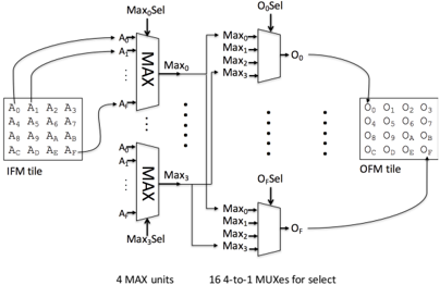
The image displays a technical block diagram of a digital circuit designed for parallel maximum value selection and routing. It illustrates a two-stage process: first, four "MAX units" process input data from an "IFM tile" (Input Feature Map), and second, sixteen 4-to-1 multiplexers (MUXes) route the results to an "OFM tile" (Output Feature Map) based on select signals. The diagram is monochrome (black lines on white background) and uses standard schematic symbols for logic blocks.
### Components/Axes
**Primary Components:**
1. **IFM tile (Left):** A 4x4 grid representing input data elements. Elements are labeled with hexadecimal subscripts:
* Row 1: A₀, A₁, A₂, A₃
* Row 2: A₄, A₅, A₆, A₇
* Row 3: A₈, A₉, Aₐ, A_b
* Row 4: A_c, A_d, A_e, A_f
2. **MAX Units (Center-Left):** Four vertically stacked rectangular blocks labeled "MAX". Each has:
* **Inputs:** Four lines from the IFM tile. The top MAX unit connects to A₀, A₁, A₂, A₃. The pattern continues for subsequent units.
* **Outputs:** A single line labeled Max₀, Max₁, Max₂, Max₃ respectively.
* **Control Input:** A line from above labeled Max₀Sel, Max₁Sel, Max₂Sel, Max₃Sel.
3. **Multiplexers (Center-Right):** Four vertically stacked 4-to-1 MUX symbols (trapezoids). Each has:
* **Data Inputs:** Four lines, one from each MAX unit output (Max₀, Max₁, Max₂, Max₃).
* **Select Input:** A line from above labeled O₀Sel, O₁Sel, O₂Sel, O₃Sel.
* **Output:** A single line labeled O₀, O₁, O₂, O₃.
4. **OFM tile (Right):** A 4x4 grid representing output data elements. Elements are labeled:
* Row 1: O₀, O₁, O₂, O₃
* Row 2: O₄, O₅, O₆, O₇
* Row 3: O₈, O₉, Oₐ, O_b
* Row 4: O_c, O_d, O_e, O_f
5. **Descriptive Text (Bottom):** "4 MAX units" and "16 4-to-1 MUXes for select".
**Spatial Grounding:**
* The IFM tile is positioned on the far left.
* The four MAX units are stacked vertically in the center-left region.
* The four MUX units are stacked vertically in the center-right region.
* The OFM tile is positioned on the far right.
* All select signals (Max_xSel, O_xSel) enter from the top of the diagram.
### Detailed Analysis
**Data Flow and Connections:**
1. **Stage 1 - Maximum Computation:** Each MAX unit receives a distinct set of four inputs from the IFM tile. For example, the top MAX unit processes {A₀, A₁, A₂, A₃}. Its function is to output the maximum value from its input set (Max₀ = max(A₀, A₁, A₂, A₃)). This is repeated in parallel for all four units, covering all 16 IFM elements.
2. **Stage 2 - Output Selection:** The outputs of all four MAX units (Max₀, Max₁, Max₂, Max₃) are fed as inputs to *each* of the four MUX units. The select signal (e.g., O₀Sel) for a given MUX determines which of the four MAX outputs is routed to its corresponding OFM element (e.g., O₀). For instance, if O₀Sel = "10" (binary), the MUX might select Max₂ to be output as O₀.
3. **Control Signals:** The diagram shows two sets of independent select controls:
* `Max_xSel`: Controls the operation of each MAX unit (possibly enabling it or selecting a specific function).
* `O_xSel`: Controls the routing selection for each output MUX.
**Component Isolation - Header (Select Signals):**
The top portion of the diagram contains all control signals. There are eight distinct select lines: Max₀Sel through Max₃Sel, and O₀Sel through O₃Sel. These are the primary control inputs that dictate the circuit's operation for a given cycle.
### Key Observations
1. **Parallelism:** The architecture is highly parallel. Four maximum operations occur simultaneously, and four output selections occur simultaneously.
2. **Interconnection Complexity:** While the diagram simplifies the wiring, it implies a dense interconnect network. Each of the 4 MUXes requires 4 input lines (from the MAX units), totaling 16 data lines between the MAX and MUX stages.
3. **Hexadecimal Labeling:** The use of hexadecimal (0-F) for subscripts in both IFM and OFM tiles is a concise way to label 16 elements (0-15 in decimal).
4. **Functional Mapping:** The circuit maps a 4x4 input block (IFM) to a 4x4 output block (OFM) through a two-step process of local maxima computation followed by configurable routing. This is characteristic of a **configurable max-pooling layer** often used in convolutional neural network (CNN) hardware accelerators.
### Interpretation
This diagram represents a hardware-optimized module for performing a **configurable 4x4 max-pooling operation**. In a CNN, max-pooling reduces the spatial dimensions of a feature map by selecting the maximum value within a window.
* **What the data suggests:** The circuit is designed for flexibility. The `Max_xSel` signals might allow the MAX units to compute different statistics (not just max), while the `O_xSel` signals allow the resulting four values to be placed into any of the 16 output positions. This could support different pooling strides or overlapping windows.
* **How elements relate:** The IFM tile is the source data. The MAX units perform the core reduction operation, condensing 16 inputs into 4 intermediate values. The MUX network then redistributes these 4 values to construct the final 16-element OFM tile, likely with zeros or other values in non-selected positions.
* **Notable Anomalies/Patterns:** The most significant pattern is the **many-to-few-to-many** data flow (16 -> 4 -> 16). This is a classic hardware efficiency pattern: reduce data to a manageable intermediate set, process it, then reconstruct the desired output shape. The separate control for MAX units and MUXes indicates a design that decouples the *computation* of features from their *placement* in the output, offering greater architectural flexibility for different neural network layers or operations.
**In essence, this is a blueprint for a specialized processing element in a AI/ML inference accelerator, designed to efficiently execute pooling operations with configurable parameters.**