## Line Chart: Efficiency vs. Semiconductor Node Size
### Overview
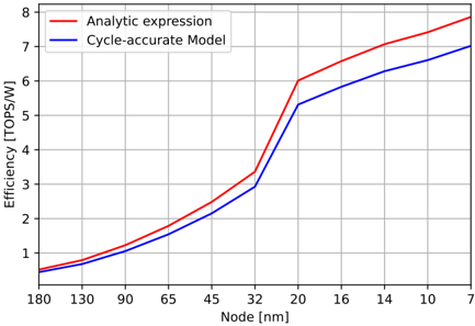
The image is a line chart comparing the computational efficiency (in TOPS/W) of two different models as a function of semiconductor manufacturing process node size (in nanometers). The chart demonstrates that efficiency increases for both models as the node size decreases (i.e., as technology advances), with the "Analytic expression" model consistently predicting higher efficiency than the "Cycle-accurate Model."
### Components/Axes
* **Chart Type:** 2D line chart with a grid.
* **X-Axis (Horizontal):**
* **Label:** `Node [nm]`
* **Scale:** Categorical, with nodes listed in descending order from left to right: `180`, `130`, `90`, `65`, `45`, `32`, `20`, `16`, `14`, `10`, `7`.
* **Note:** The spacing between categories is not linear; it appears to be roughly proportional to the inverse of the node size, emphasizing smaller nodes.
* **Y-Axis (Vertical):**
* **Label:** `Efficiency (TOPS/W)`
* **Scale:** Linear, from `0` to `8`, with major grid lines at intervals of `1`.
* **Legend:**
* **Position:** Top-left corner of the chart area.
* **Entry 1:** A solid red line labeled `Analytic expression`.
* **Entry 2:** A solid blue line labeled `Cycle-accurate Model`.
* **Grid:** A light gray grid is present, aligned with the major ticks on both axes.
### Detailed Analysis
**Trend Verification:**
* **Red Line (Analytic expression):** Slopes upward from left to right. The slope is moderate from 180 nm to 32 nm, becomes very steep between 32 nm and 20 nm, and then continues with a strong, steady upward slope from 20 nm to 7 nm.
* **Blue Line (Cycle-accurate Model):** Also slopes upward from left to right. Its slope is more consistent and gentler than the red line's, with a slight increase in steepness after 32 nm, but never as dramatic as the red line's jump.
**Data Point Extraction (Approximate Values):**
The following table reconstructs the approximate data points by reading the chart. Values are estimated based on the grid lines.
| Node [nm] | Efficiency (TOPS/W) - Analytic expression (Red) | Efficiency (TOPS/W) - Cycle-accurate Model (Blue) |
| :--- | :--- | :--- |
| 180 | ~0.6 | ~0.5 |
| 130 | ~0.8 | ~0.7 |
| 90 | ~1.2 | ~1.0 |
| 65 | ~1.8 | ~1.5 |
| 45 | ~2.5 | ~2.1 |
| 32 | ~3.3 | ~2.9 |
| 20 | ~6.0 | ~5.3 |
| 16 | ~6.4 | ~5.8 |
| 14 | ~6.9 | ~6.2 |
| 10 | ~7.4 | ~6.6 |
| 7 | ~7.9 | ~7.0 |
**Spatial Grounding & Key Relationships:**
* The red line is positioned above the blue line across the entire chart, indicating the Analytic expression model always estimates higher efficiency.
* The vertical gap between the two lines is smallest at the largest node (180 nm) and widens significantly as node size decreases, particularly after the 32 nm point.
* The most notable feature is the sharp "knee" or inflection point in the red line between 32 nm and 20 nm, where its efficiency nearly doubles. The blue line shows a much more subdued increase in this region.
### Key Observations
1. **Consistent Positive Correlation:** For both models, efficiency (TOPS/W) improves as the semiconductor node size shrinks.
2. **Diverging Predictions:** The discrepancy between the two models grows with technological advancement. The Analytic expression becomes increasingly optimistic relative to the Cycle-accurate Model at smaller nodes.
3. **Critical Transition Region:** The node range between 32 nm and 20 nm is a critical transition point, especially for the Analytic expression, which predicts a dramatic efficiency leap.
4. **Monotonic Increase:** Both data series are strictly monotonic; there are no dips or decreases in efficiency as nodes get smaller.
### Interpretation
This chart likely compares a theoretical, formula-based model ("Analytic expression") of chip efficiency against a more detailed, simulation-based model ("Cycle-accurate Model"). The data suggests that while both agree on the general trend of improving efficiency with scaling, the theoretical model is more aggressive in its predictions.
The widening gap implies that the cycle-accurate model accounts for real-world overheads, complexities, or diminishing returns that the analytic expression simplifies or ignores. The dramatic jump in the analytic curve around 20 nm could represent a theoretical threshold where a new architectural or physical paradigm (e.g., a shift in transistor design or interconnect technology) is assumed to unlock massive gains. The cycle-accurate model, being more grounded in detailed simulation, shows a more gradual, realistic improvement.
**In essence, the chart visualizes the difference between an idealized projection and a more nuanced simulation of semiconductor scaling benefits.** It serves as a caution that theoretical models may overestimate gains, and detailed modeling is crucial for accurate forecasting in advanced technology nodes.