## Diagram: Transistor Structure and Capacitance Model
### Overview
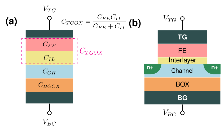
The image presents two technical diagrams illustrating a transistor structure and its associated capacitance model. Diagram (a) shows a vertical stack of labeled components with a capacitance formula, while diagram (b) depicts the physical layer structure of the transistor with n+ regions and voltage annotations.
### Components/Axes
**Diagram (a):**
- **Vertical Stack Components (Left to Right):**
- Top: Dark green block labeled **TG** (Top Gate)
- Red block labeled **FE** (Fixed Electrode)
- Yellow block labeled **IL** (Interlayer)
- Light blue block labeled **CH** (Channel)
- Orange block labeled **BOX** (Buried Oxide)
- Bottom: Dark green block labeled **BG** (Bulk Gate)
- **Voltage Labels:**
- Top: **V_TG** (Top Gate Voltage)
- Bottom: **V_BG** (Bulk Gate Voltage)
- **Capacitance Labels:**
- **C_FE**, **C_IL**, **C_CH**, **C_BGOX** (capacitances of respective components)
- **C_TGOX** (total gate oxide capacitance) with formula:
**C_TGOX = (C_FE * C_IL) / (C_FE + C_IL)**
**Diagram (b):**
- **Vertical Stack Components (Top to Bottom):**
- **TG** (Top Gate)
- **FE** (Fixed Electrode)
- **Interlayer**
- **Channel** (with **n+** regions on both sides)
- **BOX** (Buried Oxide)
- **BG** (Bulk Gate)
- **Voltage Labels:**
- Top: **V_TG**
- Bottom: **V_BG**
### Detailed Analysis
**Diagram (a):**
- The capacitance model breaks down the total gate oxide capacitance (**C_TGOX**) into contributions from the fixed electrode (**C_FE**) and interlayer (**C_IL**). The formula represents a parallel capacitance combination.
- Colors are used to differentiate components: red (FE), yellow (IL), blue (CH), orange (BOX), and dark green (TG/BG).
**Diagram (b):**
- Physical transistor structure with distinct layers:
- **TG** (Top Gate) and **FE** (Fixed Electrode) form the gate stack.
- **Interlayer** separates the gate stack from the **Channel**, which includes **n+** regions (source/drain).
- **BOX** (Buried Oxide) and **BG** (Bulk Gate) complete the structure.
### Key Observations
1. **Capacitance Model (a):**
- **C_TGOX** is derived from the parallel combination of **C_FE** and **C_IL**, indicating these components contribute additively to the total gate oxide capacitance.
- The **CH** (Channel) and **BOX** (Buried Oxide) are distinct from the gate oxide components.
2. **Physical Structure (b):**
- The **n+** regions flank the **Channel**, typical of MOSFET source/drain regions.
- The **BOX** layer underlies the **Channel**, separating it from the **BG** (Bulk Gate).
### Interpretation
- **Relationship Between Diagrams:**
Diagram (a) provides an electrical model of capacitance distribution, while diagram (b) shows the physical layout. The **FE** and **IL** components in (a) correspond to the **FE** (Fixed Electrode) and **Interlayer** in (b), respectively.
- **Functional Insights:**
- The **n+** regions in (b) suggest a p-channel or n-channel configuration depending on doping.
- The **BOX** layer in (b) aligns with the **BOX** capacitance in (a), acting as a substrate for the channel.
- The formula for **C_TGOX** implies that increasing either **C_FE** or **C_IL** would proportionally increase the total gate oxide capacitance, critical for device performance.
- **Design Implications:**
The separation of **FE** and **IL** capacitances allows optimization of gate oxide properties. The **n+** regions in (b) ensure low-resistance contacts for current flow.
No numerical values or trends are provided beyond the formula. The diagrams focus on structural and electrical relationships rather than quantitative data.