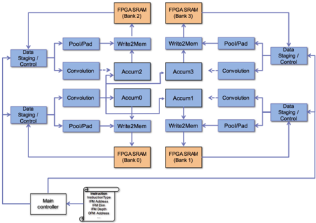
## Diagram: FPGA Data Flow
### Overview
The image is a block diagram illustrating the data flow within an FPGA-based system, likely for image processing or similar applications. It shows the interconnection of various processing blocks, memory banks, and a main controller.
### Components/Axes
* **Blocks:** The diagram consists of rectangular blocks representing functional units. These blocks are colored blue, except for the FPGA SRAM blocks, which are orange.
* **Arrows:** Blue arrows indicate the direction of data flow between the blocks. Dashed arrows are also present.
* **Text Labels:** Each block is labeled with its function (e.g., "Data Staging/Control", "Convolution", "Pool/Pad", "Write2Mem", "Accum").
* **Memory Banks:** Four FPGA SRAM blocks are labeled as Bank 0, Bank 1, Bank 2, and Bank 3.
* **Main Controller:** A block labeled "Main controller" is present at the bottom-left.
* **Instruction Box:** A box near the main controller contains the word "Instruction" and the following parameters: "InstructionType", "IFM Address", "IFM Dim", "IFM Depth", "OFM Address".
### Detailed Analysis
* **Data Staging/Control:** There are four "Data Staging/Control" blocks, one at each corner of the central processing array.
* **Convolution:** There are two pairs of "Convolution" blocks.
* **Pool/Pad:** There are two pairs of "Pool/Pad" blocks.
* **Write2Mem:** There are two pairs of "Write2Mem" blocks.
* **Accum:** There are four "Accum" blocks, labeled Accum0, Accum1, Accum2, and Accum3.
* **FPGA SRAM:** The four FPGA SRAM blocks are positioned at the top and bottom of the diagram. Bank 2 and Bank 3 are at the top, while Bank 0 and Bank 1 are at the bottom.
* **Data Flow:**
* Data flows from the "Data Staging/Control" blocks to "Pool/Pad" and "Convolution" blocks.
* "Pool/Pad" blocks feed into "Write2Mem" blocks.
* "Convolution" blocks feed into "Accum" blocks.
* "Write2Mem" blocks write to the FPGA SRAM banks.
* Data flows from the FPGA SRAM banks back to the "Data Staging/Control" blocks.
* The "Main controller" connects to all "Data Staging/Control" blocks.
* Dashed arrows connect the "Convolution" blocks to the "Accum" blocks.
### Key Observations
* The diagram represents a parallel processing architecture.
* The data flow is cyclical, with data being processed and stored in memory before being fed back into the processing pipeline.
* The "Main controller" likely manages the overall operation of the system.
### Interpretation
The diagram illustrates a hardware architecture implemented on an FPGA for performing a series of operations, likely related to image processing or deep learning. The "Convolution" blocks suggest convolutional neural network processing. The "Pool/Pad" blocks suggest pooling and padding operations commonly used in CNNs. The data flow indicates that data is staged, processed, stored in memory, and then reused. The parallel structure suggests that the architecture is designed for high-throughput processing. The instruction box suggests that the main controller is responsible for configuring the processing pipeline.