\n
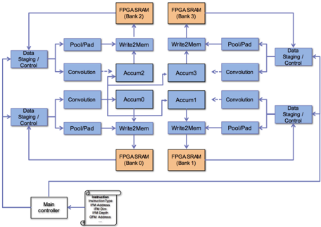
## Diagram: Convolutional Neural Network Architecture on FPGA
### Overview
The image depicts a diagram of a convolutional neural network (CNN) architecture implemented on a Field-Programmable Gate Array (FPGA). The diagram illustrates the data flow between various processing units (Convolution, PoolPad, Accum) and memory banks (FPGA SRAM). The architecture appears to be designed for parallel processing, with multiple instances of convolution and accumulation units operating concurrently.
### Components/Axes
The diagram consists of the following key components:
* **Main Controller:** Located at the bottom-left, providing instructions.
* **Data Staging / Control:** Located on the left and right sides, managing data input and output.
* **FPGA SRAM (Bank 0, Bank 1, Bank 2, Bank 3):** Four memory banks, positioned in the corners, storing data.
* **PoolPad:** Units for pooling and padding operations.
* **Convolution:** Units for convolutional operations.
* **Accum0, Accum1, Accum2, Accum3:** Accumulation units.
* **Write2Mem:** Units for writing data to memory.
* **Instruction Block:** A small block connected to the Main Controller, containing the following labels:
* Instruction
* InstructionType
* IFM Address
* IFM Size
* OFM Depth
* OFM Address
### Detailed Analysis or Content Details
The diagram shows a data flow starting from the "Data Staging / Control" blocks on the left. The data is then split into multiple parallel paths.
1. **Top Path:**
* Data flows from "Data Staging / Control" to "PoolPad".
* "PoolPad" outputs to "Write2Mem".
* "Write2Mem" writes to "FPGA SRAM (Bank 2)".
* Data flows from "FPGA SRAM (Bank 2)" to "Convolution".
* "Convolution" outputs to "Accum2".
* "Accum2" outputs to "Convolution".
* "Convolution" outputs to "PoolPad".
* "PoolPad" outputs to "Data Staging / Control".
2. **Middle Path:**
* Data flows from "Data Staging / Control" to "Convolution".
* "Convolution" outputs to "Accum0".
* "Accum0" outputs to "Convolution".
* "Convolution" outputs to "Accum1".
* "Accum1" outputs to "Convolution".
* "Convolution" outputs to "PoolPad".
* "PoolPad" outputs to "Data Staging / Control".
3. **Bottom Path:**
* Data flows from "Data Staging / Control" to "PoolPad".
* "PoolPad" outputs to "Write2Mem".
* "Write2Mem" writes to "FPGA SRAM (Bank 0)".
* Data flows from "FPGA SRAM (Bank 0)" to "Convolution".
* "Convolution" outputs to "Accum2".
* "Accum2" outputs to "Convolution".
* "Convolution" outputs to "PoolPad".
* "PoolPad" outputs to "Data Staging / Control".
4. **Right Path:**
* Data flows from "Data Staging / Control" to "PoolPad".
* "PoolPad" outputs to "Write2Mem".
* "Write2Mem" writes to "FPGA SRAM (Bank 3)".
* Data flows from "FPGA SRAM (Bank 3)" to "Convolution".
* "Convolution" outputs to "Accum3".
* "Accum3" outputs to "Convolution".
* "Convolution" outputs to "PoolPad".
* "PoolPad" outputs to "Data Staging / Control".
The "Main Controller" is connected to the "Instruction" block, which provides control signals to the entire system. The connections between the components are represented by arrows indicating the direction of data flow.
### Key Observations
* The architecture is highly parallel, with multiple convolution and accumulation units operating simultaneously.
* The use of FPGA SRAM banks suggests a distributed memory architecture.
* The "PoolPad" units are strategically placed to perform pooling and padding operations.
* The "Write2Mem" units are used to store intermediate results in the FPGA SRAM banks.
* The "Data Staging / Control" blocks manage the flow of data into and out of the system.
### Interpretation
This diagram illustrates a hardware implementation of a CNN on an FPGA. The parallel architecture is designed to accelerate the computationally intensive convolution and accumulation operations. The use of FPGA SRAM banks allows for efficient storage and retrieval of data. The "Main Controller" provides the necessary control signals to orchestrate the entire process. The diagram suggests a pipelined architecture, where data flows through the various processing units in a sequential manner. The design aims to maximize throughput and minimize latency, making it suitable for real-time applications such as image recognition and object detection. The instruction block suggests the system is programmable, allowing for flexibility in configuring the CNN architecture. The diagram does not provide specific numerical values or performance metrics, but it clearly demonstrates the overall structure and data flow of the system. The arrangement of the components suggests a focus on maximizing data reuse and minimizing memory access, which are critical for achieving high performance on an FPGA.