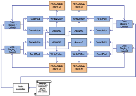
## Hardware Architecture Diagram: FPGA-Based Parallel Processing System
### Overview
The image displays a technical block diagram of a parallel processing architecture, likely designed for an FPGA (Field-Programmable Gate Array). The system features a symmetrical, four-quadrant design centered around accumulation units, with data flow managed by staging controllers and results stored in dedicated SRAM banks. A main controller oversees operations via an instruction memory interface.
### Components/Axes
The diagram is composed of interconnected functional blocks, color-coded by type:
* **Blue Blocks (Data Staging / Control):** Positioned on the far left and right edges. Two are on the left side, and two are on the right side, serving as the primary data ingress/egress points.
* **Light Blue Blocks (Processing Units):** These form the core computational pipeline within each quadrant.
* `PoolPad`: Likely performs pooling and padding operations.
* `Convolution`: Executes convolution operations.
* `Accum0`, `Accum1`, `Accum2`, `Accum3`: Accumulator units located at the center of the diagram, forming a 2x2 grid.
* `Write2Mem`: Memory write interface blocks.
* **Orange Blocks (Memory):**
* `FPGA SRAM (Bank 0)`: Located at the bottom-center.
* `FPGA SRAM (Bank 1)`: Located at the bottom-right.
* `FPGA SRAM (Bank 2)`: Located at the top-center.
* `FPGA SRAM (Bank 3)`: Located at the top-right.
* **Gray Blocks (Control & Instruction):**
* `Main controller`: Positioned at the bottom-left corner.
* `Instruction Memory`: A block connected to the Main controller, containing the following text labels:
* `Instructions`
* `Instruction Address`
* `Instructions Data`
* `Data Address`
### Detailed Analysis
**Data Flow & Connectivity:**
The architecture exhibits a clear, symmetrical data flow pattern.
1. **Input/Output:** Data enters and exits the system through the four `Data Staging / Control` blocks on the left and right peripheries.
2. **Processing Path (Per Quadrant):** From a staging block, data flows inward through a `PoolPad` unit and a `Convolution` unit. The outputs from these processing units are directed to the central `Accum` blocks.
3. **Accumulation & Storage:** The four `Accum` units (`Accum0` to `Accum3`) are interconnected in the center. Their outputs are routed to `Write2Mem` blocks.
4. **Memory Interface:** Each `Write2Mem` block is connected to a specific `FPGA SRAM` bank:
* `Accum0` -> `Write2Mem` -> `FPGA SRAM (Bank 0)`
* `Accum1` -> `Write2Mem` -> `FPGA SRAM (Bank 1)`
* `Accum2` -> `Write2Mem` -> `FPGA SRAM (Bank 2)`
* `Accum3` -> `Write2Mem` -> `FPGA SRAM (Bank 3)`
5. **Global Control:** The `Main controller` at the bottom-left is connected to all four `Data Staging / Control` blocks and the `Instruction Memory`, indicating it orchestrates the entire process by issuing commands and managing data flow.
**Spatial Layout:**
* **Top Half:** Contains `Data Staging / Control` (top-left, top-right), `PoolPad`, `Convolution`, `Accum2`, `Accum3`, `Write2Mem`, and `FPGA SRAM (Bank 2 & 3)`.
* **Bottom Half:** Contains `Data Staging / Control` (bottom-left, bottom-right), `PoolPad`, `Convolution`, `Accum0`, `Accum1`, `Write2Mem`, `FPGA SRAM (Bank 0 & 1)`, the `Main controller`, and the `Instruction Memory`.
* **Central Core:** The 2x2 grid of `Accum` units (`Accum0-3`) forms the heart of the diagram.
### Key Observations
1. **Symmetry and Parallelism:** The design is highly symmetrical, suggesting a parallel processing architecture where four similar data paths operate concurrently. This is typical for accelerating workloads like neural network inference, where convolution and pooling are key operations.
2. **Dedicated Memory Banks:** Each accumulator has a dedicated SRAM bank, preventing memory access bottlenecks and enabling high-bandwidth, parallel write operations.
3. **Hierarchical Control:** A single `Main controller` manages multiple `Data Staging / Control` units, indicating a hierarchical control structure where high-level instructions are decomposed into localized control signals.
4. **Instruction-Driven Operation:** The presence of an `Instruction Memory` block confirms this is a programmable architecture, not a fixed-function circuit. The controller fetches instructions to determine the sequence of operations.
### Interpretation
This diagram represents a **specialized, parallel compute array** optimized for data-intensive, regular operations like those found in convolutional neural networks (CNNs) or image processing pipelines.
* **What it demonstrates:** The architecture is designed for high throughput by processing multiple data streams in parallel (four quadrants). The `Convolution` and `PoolPad` blocks are telltale signs of a deep learning or computer vision accelerator. The central `Accum` units suggest a reduction step, common after convolution operations to sum partial products.
* **Relationships:** The `Main controller` is the brain, the `Data Staging` units are the limbs handling I/O, the `Convolution`/`PoolPad` blocks are the specialized muscles performing core computations, and the `FPGA SRAM` banks are the fast, local memory for intermediate results. The `Instruction Memory` provides the programmability, allowing this hardware to be configured for different algorithms.
* **Notable Design Choices:** The strict separation of memory banks per accumulator is a critical design choice to maximize memory bandwidth and avoid contention, which is often the bottleneck in parallel systems. The symmetrical layout likely maps efficiently onto the FPGA's physical fabric, optimizing place-and-route results for performance and power efficiency.
**Language Declaration:** All text in the image is in English.