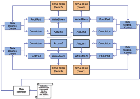
## Block Diagram: FPGA-Based Data Processing Pipeline
### Overview
The diagram illustrates a modular data processing architecture for an FPGA (Field-Programmable Gate Array) system. It depicts data flow between memory banks, processing units, and control logic, emphasizing parallelism and iterative computation. The system includes four FPGA SRAM banks (0-3), data staging/control modules, pooling/padding units, memory write operations, accumulation stages, and convolution layers.
### Components/Axes
- **FPGA SRAM Banks**: Four memory banks labeled "FPGA SRAM (Bank 0)" to "FPGA SRAM (Bank 3)" in orange.
- **Data Staging/Control**: Blue blocks on the left and right edges, acting as input/output interfaces.
- **Pool/Pad**: Blue blocks connected to Data Staging/Control and Convolution units.
- **Write2Mem**: Blue blocks linking Pool/Pad to Accumulation stages.
- **Accumulation Stages**: Four blocks labeled "Accum0" to "Accum3" in the center.
- **Convolution**: Blue blocks connected to Accumulation stages and Pool/Pad.
- **Main Controller**: A white block at the bottom-left, sending instructions to FPGA SRAM banks.
### Detailed Analysis
1. **Data Flow Path**:
- **Input**: Data enters via "Data Staging/Control" on the left, flows through Pool/Pad, then Write2Mem to Accumulation stages (Accum0-3).
- **Processing**: Accumulation stages feed into Convolution units, which loop back to Pool/Pad and Data Staging/Control.
- **Output**: Processed data exits via "Data Staging/Control" on the right.
2. **FPGA SRAM Banks**:
- Banks 0-3 are arranged in a 2x2 grid, with Bank 0 at the bottom-left and Bank 3 at the top-right.
- Each bank receives instructions from the Main Controller, specifying parameters like `InstructionType`, `IFM Address`, `IFM Dim`, `IFM Depth`, and `OFM Address`.
3. **Control Logic**:
- The Main Controller orchestrates operations by sending structured instructions to FPGA SRAM banks.
- Feedback loops from Convolution to Pool/Pad and Data Staging/Control suggest iterative or recurrent processing.
### Key Observations
- **Parallelism**: Four SRAM banks enable concurrent data storage/retrieval.
- **Modular Design**: Components are decoupled, allowing scalability (e.g., adding more Accumulation/Convolution stages).
- **Feedback Mechanism**: Convolution outputs re-enter the pipeline, indicating support for recurrent neural networks or iterative algorithms.
### Interpretation
This architecture is optimized for high-throughput, parallel data processing, likely for machine learning workloads (e.g., convolutional neural networks). The Main Controller’s instruction set implies programmability, allowing customization of data dimensions (`IFM Dim`, `IFM Depth`) and output formats (`OFM Address`). The feedback loop suggests the system can handle temporal or spatial dependencies in data, critical for tasks like video processing or recurrent networks. The use of FPGA SRAM banks highlights a focus on low-latency, hardware-accelerated computation.